EL8171FSZ-T7 查看數據表(PDF) - Intersil
零件编号
产品描述 (功能)
生产厂家
EL8171FSZ-T7 Datasheet PDF : 14 Pages
| |||
EL8171, EL8172
Gain Setting
VIN, the potential difference across IN+ and IN-, is replicated
(less the input offset voltage) across FB+ and FB-. The
obsession of the EL8171 and EL8172 in-amp is to maintain
the differential voltage across FB+ and FB- equal to IN+ and
IN-; (FB+ - FB-) = (IN+ - IN-). Consequently, the transfer
function can be derived. The gain of the EL8171 and EL8172
is set by two external resistors, the feedback resistor RF, and
the gain resistor RG.
2.4V TO 5.5V
VIN/2
VCM
VIN/2
71
3 IN+
V+
+
2 IN-
-
8 FB+ EL8171/2
6
+
5 FB- -
V-
4
VOUT
RG
RF
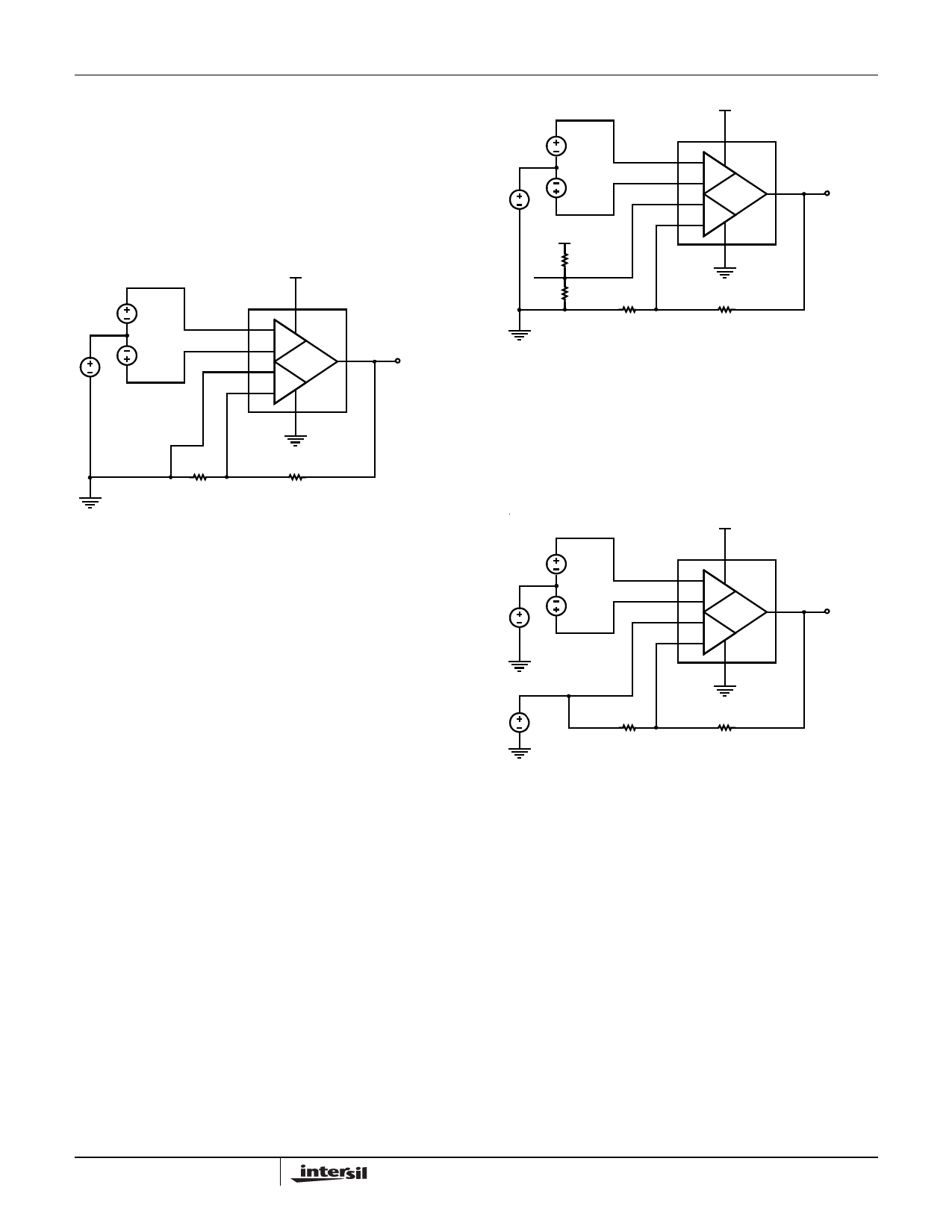
FIGURE 37. CIRCUIT 1 - GAIN IS BY EXTERNAL RESISTORS
RF AND RG
VOUT
=
⎛
⎜1
⎝
+
R-R----G-F--⎠⎟⎞
VIN
(EQ. 1)
In Figure 37, the FB+ pin and one end of resistor RG are
connected to GND. With this configuration, Equation 1 is
only true for a positive swing in VIN; negative input swings
will be ignored and the output will be at ground.
Reference Connection
Unlike a three-op amp instrumentation amplifier, a finite
series resistance seen at the REF terminal does not degrade
the EL8171 and EL8172's high CMRR performance,
eliminating the need for an additional external buffer
amplifier. Circuit 2 (Figure 38) uses the FB+ pin to provide a
high impedance REF terminal.
The FB+ pin is used as a REF terminal to center or to adjust
the output. Because the FB+ pin is a high impedance input,
an economical resistor divider can be used to set the voltage
at the REF terminal without degrading or affecting the CMRR
performance. Any voltage applied to the REF terminal will
shift VOUT by VREF times the closed loop gain, which is set
by resistors RF and RG. See Circuit 2 (Figure 38). Note that
any noise or unwanted signals on the reference supply will
be amplified at the output according to Equation 2.
The FB+ pin can also be connected to the other end of resistor,
RG. See Circuit 3 (Figure 39). Keeping the basic concept that
the EL8171 and EL8172 in-amps maintain constant differential
voltage across the input terminals and feedback terminals (IN+
- IN- = FB+ - FB-), the transfer function of Circuit 3 can be
derived. Note that the VREF gain term is eliminated and
VIN/2
VIN/2
VCM
2.4V TO 5.5V
R1
REF
R2
RG
2.4V TO 5.5V
71
3 IN+
V+
+
2 IN-
-
8 FB+ EL8171/2
6
+
5 FB- -
V-
4
RF
VOUT
FIGURE 38. CIRCUIT 2 - GAIN SETTING AND REFERENCE
CONNECTION
VOUT
=
⎛
⎜
⎝
1
+
R-R----G-F--⎠⎟⎞
(VIN
)
+
⎛
⎜
⎝
1
+
R-R----G-F--⎠⎟⎞
(
VREF
)
(EQ. 2)
susceptibility to external noise is reduced, however the VREF
source must be capable of sourcing or sinking the feedback
current from VOUT through RF and RG.
2.4V TO 5.5V
VIN/2
VCM
VIN/2
71
3 IN+
V+
+
2 IN-
-
8 FB+ EL8171/2
6
+
5 FB-
- V-
4
VOUT
RG
RF
VREF
FIGURE 39. CIRCUIT 3 - REFERENCE CONNECTION WITH AN
AVAILABLE VREF
VOUT
=
⎛
⎜
⎝
1
+
R-R----G-F--⎠⎟⎞
(VIN
)
+
(
VREF
)
External Resistor Mismatches
(EQ. 3)
Because of the independent pair of feedback terminals
provided by the EL8171 and EL8172, the CMRR is not
degraded by any resistor mismatches. Hence, unlike a three op
amp and especially a two op amp in-amp, the EL8171 and
EL8172 reduce the cost of external components by allowing the
use of 1% or more tolerance resistors without sacrificing CMRR
performance. The EL8171 and EL8172 CMRR will be
maintained regardless of the tolerance of the resistors used.
Gain Error and Accuracy
The EL8172 has a Gain Error (EG) of 0.2% typical. The
EL8171 has an EG of 0.15% typical. The gain error indicated
in the “Electrical Specifications” table on page 2 is the inherent
gain error of the EL8171 and EL8172 and does not include
11
FN6293.5
July 27, 2009
Share Link: 