2N6030 查看數據表(PDF) - Inchange Semiconductor
零件编号
产品描述 (功能)
生产厂家
2N6030 Datasheet PDF : 3 Pages
| |||
Inchange Semiconductor
Silicon PNP Power Transistors
Product Specification
2N6029 2N6030
DESCRIPTION
·With TO-3 package
·Complement to type 2N5629 2N5630
·High power dissipations
APPLICATIONS
·For high voltage and high power
amplifier applications
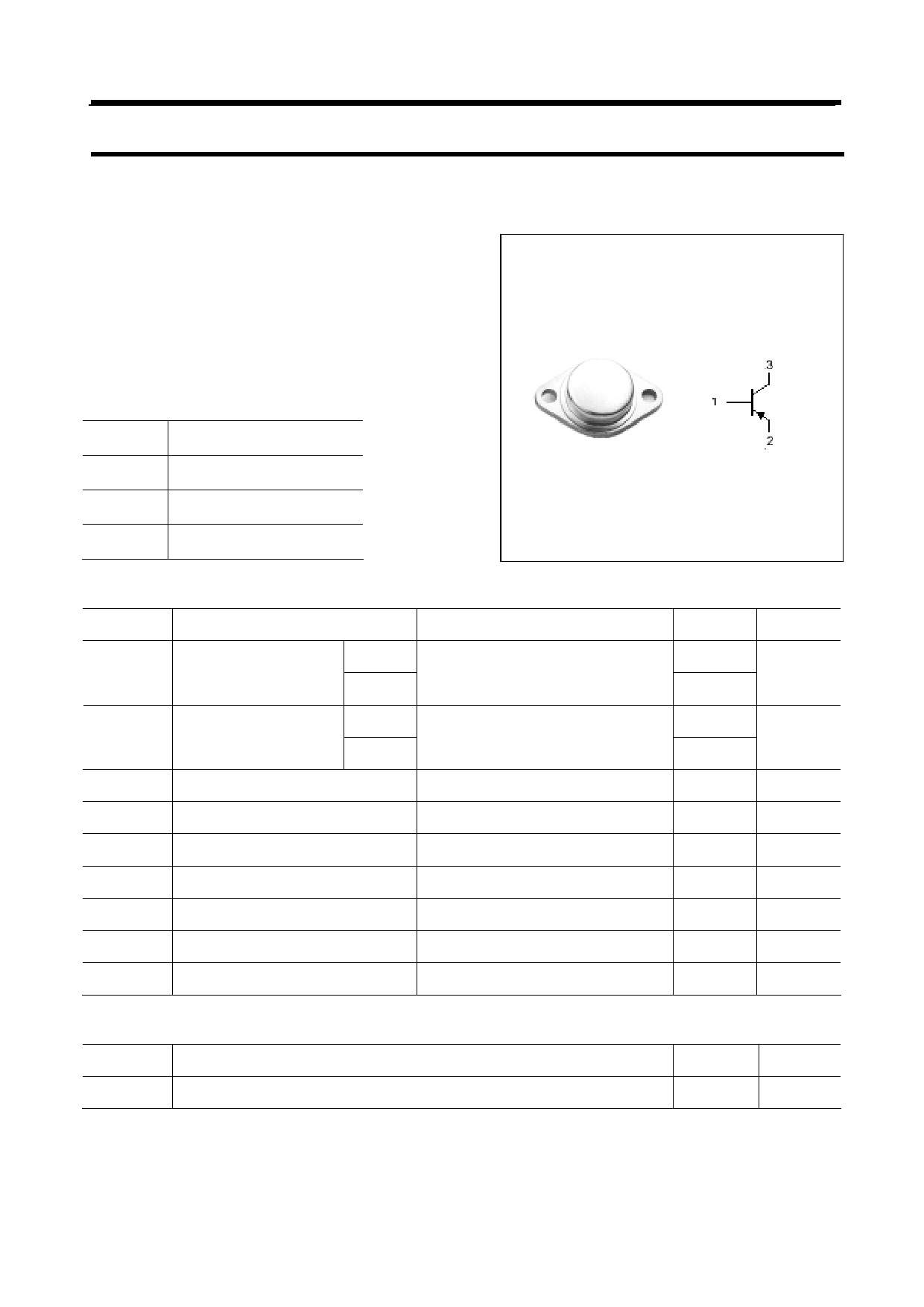
PINNING
PIN
1
2
3
DESCRIPTION
Base
Emitter
Collector
Fig.1 simplified outline (TO-3) and symbol
Absolute maximum ratings(Ta=℃)
SYMBOL
PARAMETER
VCBO
Collector-base voltage
2N6029
2N6030
VCEO
Collector-emitter voltage
2N6029
2N6030
VEBO
Emitter-base voltage
IC
Collector current
ICM
Collector current-peak
IB
Base current
PD
Total Power Dissipation
Tj
Junction temperature
Tstg
Storage temperature
CONDITIONS
Open emitter
Open base
Open collector
TC=25℃
VALUE
-100
-120
-100
-120
-7
-16
-20
-5.0
200
150
-65~200
UNIT
V
V
V
A
A
A
W
℃
℃
THERMAL CHARACTERISTICS
SYMBOL
PARAMETER
Rth j-c
Thermal resistance junction to case
VALUE
0.875
UNIT
℃/W
Share Link: 