ADF7020 查看數據表(PDF) - Analog Devices
零件编号
产品描述 (功能)
生产厂家
ADF7020 Datasheet PDF : 48 Pages
| |||
ADF7020
ABSOLUTE MAXIMUM RATINGS
TA = 25°C, unless otherwise noted.
Table 3.
Parameter
VDD to GND1
Analog I/O Voltage to GND
Digital I/O Voltage to GND
Operating Temperature Range
Industrial (B Version)
Storage Temperature Range
Maximum Junction Temperature
MLF θJA Thermal Impedance
Reflow Soldering
Peak Temperature
Time at Peak Temperature
Rating
−0.3 V to +5 V
−0.3 V to AVDD + 0.3 V
−0.3 V to DVDD + 0.3 V
−40°C to +85°C
−65°C to +125°C
150°C
26°C/W
260°C
40 sec
1 GND = GND1 = RFGND = GND4 = VCO GND = 0 V.
Data Sheet
Stresses above those listed under Absolute Maximum Ratings
may cause permanent damage to the device. This is a stress
rating only; functional operation of the device at these or any
other conditions above those indicated in the operational
section of this specification is not implied. Exposure to absolute
maximum rating conditions for extended periods may affect
device reliability.
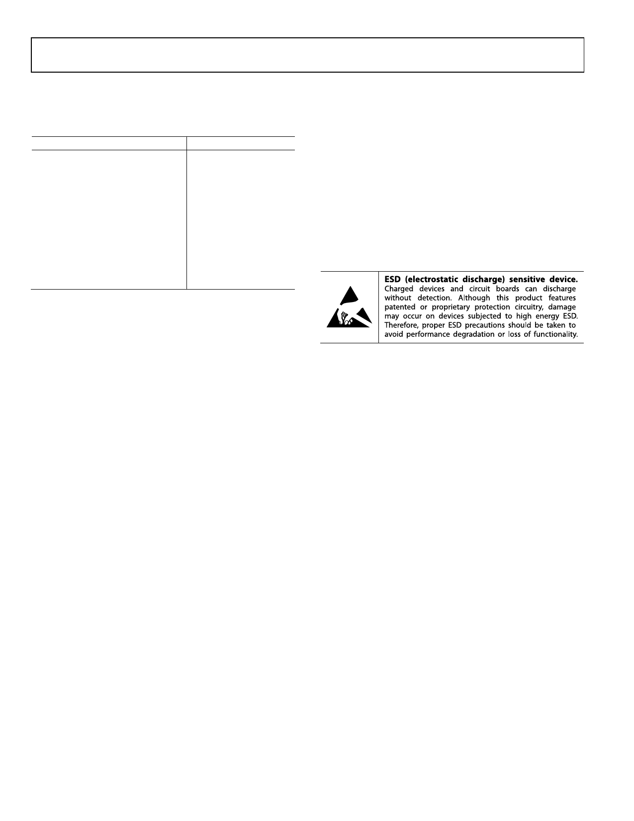
This device is a high performance RF integrated circuit with an
ESD rating of <2 kV, and is ESD sensitive. Proper precautions
should be taken for handling and assembly.
ESD CAUTION
Rev. D | Page 10 of 48
Share Link: 