ADM8828 查看數據表(PDF) - Analog Devices
零件编号
产品描述 (功能)
生产厂家
ADM8828 Datasheet PDF : 6 Pages
| |||
ADM8828/ADM8829–SPECIFICATIONS (VIN = +5 V, C1, C2 = 1 F,1 TA = TMIN to TMAX unless other-
wise noted)
Parameter
Min
Typ
Max
Input Voltage, IN
1.5
5.5
Supply Current
600
1000
Output Current
Output Resistance
Output Ripple
25
18
28
25
130
Charge-Pump Frequency
50
120
190
65
Power Efficiency
Voltage Conversion Efficiency
90
87
99.5
99.96
98
91
Shutdown Supply Current, ISHDN
Shutdown Input Voltage, VSHDN
Shutdown Exit Time
0.02
2
2.0
0.8
175
NOTES
1C1 and C2 are low ESR (<0.2 Ω) electrolytic capacitors. High ESR will degrade performance.
Specifications subject to change without notice.
Units
V
µA
mA
Ω
mV p-p
mV p-p
kHz
kHz
%
%
%
%
%
µA
V
V
µs
Test Conditions/Comments
RL = 10 kΩ
Unloaded
IL = 5 mA
IL = 5 mA
IL = 25 mA
VIN = +2.25 V
RL = 200 Ω
RL = 1 kΩ
No Load
RL = 1 kΩ
RL = 200 Ω
SHDN = IN
SHDN High = Disabled
SHDN Low = Enabled
IL = 5 mA
ABSOLUTE MAXIMUM RATINGS*
(TA = +25°C unless otherwise noted)
Input Voltage (IN to GND) . . . . . . . . . . . . . . . –0.3 V to +6 V
OUT to GND . . . . . . . . . . . . . . . . . . . . . . . . –6.0 V to +0.3 V
OUT, IN Output Current (Continuous) . . . . . . . . . . . . 50 mA
Output Short Circuit Duration to GND . . . . . . . . . . . 10 secs
Power Dissipation, RT-6 . . . . . . . . . . . . . . . . . . . . . . 570 mW
(Derate 8.3 mW/°C above +70°C)
θJA, Thermal Impedance . . . . . . . . . . . . . . . . . . . . 120°C/W
Operating Temperature Range
Industrial (A Version) . . . . . . . . . . . . . . . . – 40°C to +85°C
Storage Temperature Range . . . . . . . . . . . –65°C to +150°C
Lead Temperature Range (Soldering 10 sec) . . . . . . . . +300°C
Vapor Phase (70 sec) . . . . . . . . . . . . . . . . . . . . . . . . +215°C
Infrared (15 sec) . . . . . . . . . . . . . . . . . . . . . . . . . . . . +220°C
ESD Rating . . . . . . . . . . . . . . . . . . . . . . . . . . . . . . . . >3500 V
*This is a stress rating only and functional operation of the device at these or any
other conditions above those indicated in the operation section of this specification
is not implied. Exposure to absolute maximum rating conditions for extended
periods may affect device reliability.
ORDERING GUIDE
Model
Temperature
Range
ADM8828ART –40°C to +85°C
ADM8829ART –40°C to +85°C
*RT-6 = 6-lead SOT-23.
Branding
Information
MM0
MN0
Package
Option*
RT-6
RT-6
PIN FUNCTION DESCRIPTIONS
Mnemonic
CAP+
GND
CAP–
OUT
SHDN
IN
Function
Positive Charge-Pump Capacitor Terminal.
Power Supply Ground.
Negative Charge-Pump Capacitor Terminal.
Output, Negative Voltage.
Shutdown Control Input. This input, when
high, is used to disable the charge pump
thereby reducing the power consumption.
Positive Power Supply Input.
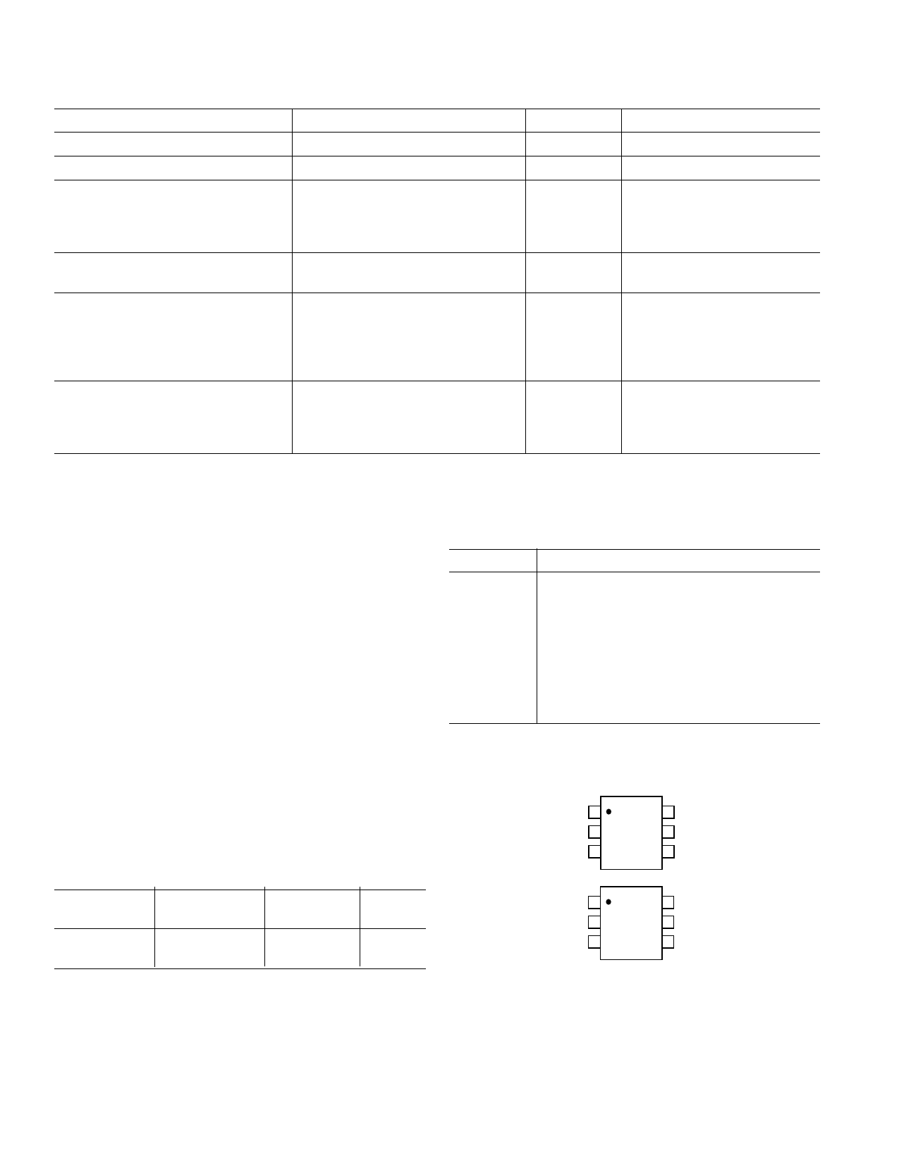
PIN CONFIGURATIONS
OUT 1
6 CAP+
ADM8828
IN 2 TOP VIEW 5 SHDN
CAP– 3 (Not to Scale) 4 GND
OUT 1
6 CAP+
ADM8829
IN 2 TOP VIEW 5 NC
CAP– 3 (Not to Scale) 4 GND
NC = NO CONNECT
–2–
REV. A
Share Link: 