CAT64LC40Y-GT3 查看數據表(PDF) - ON Semiconductor
零件编号
产品描述 (功能)
生产厂家
CAT64LC40Y-GT3 Datasheet PDF : 12 Pages
| |||
CAT64LC40
Table 6. POWER−UP TIMING (Notes 8 and 9)
Symbol
Parameter
Min
Max
tPUR
Power−Up to Read Operation
10
tPUW
Power−Up to Program Operation
1
8. This parameter is tested initially and after a design or process change that affects the parameter.
9. tPUR and tPUW are the delays required from the time VCC is stable until the specified operation can be initiated.
Table 7. WRITE CYCLE LIMITS
Symbol
tWR
Program Cycle Time
Parameter
Min
Max
2.5 V
10
4.5 V − 6.0 V
5
Units
ms
ms
Units
ms
Table 8. INSTRUCTION SET
Instruction
Opcode
Address
Data
Read
10101000
A7 A6 A5 A4 A3 A2 A1 A0
D15 − D0
Write
10100100
A7 A6 A5 A4 A3 A2 A1 A0
D15 − D0
Write Enable
10100011
XXXXXXXX
Write Disable
10100000
XXXXXXXX
[Write All Locations] (Note 10)
10100001
XXXXXXXX
D15 − D0
10. (Write All Locations) is a test mode operation and is therefore not included in the AC/DC Operations specifications.
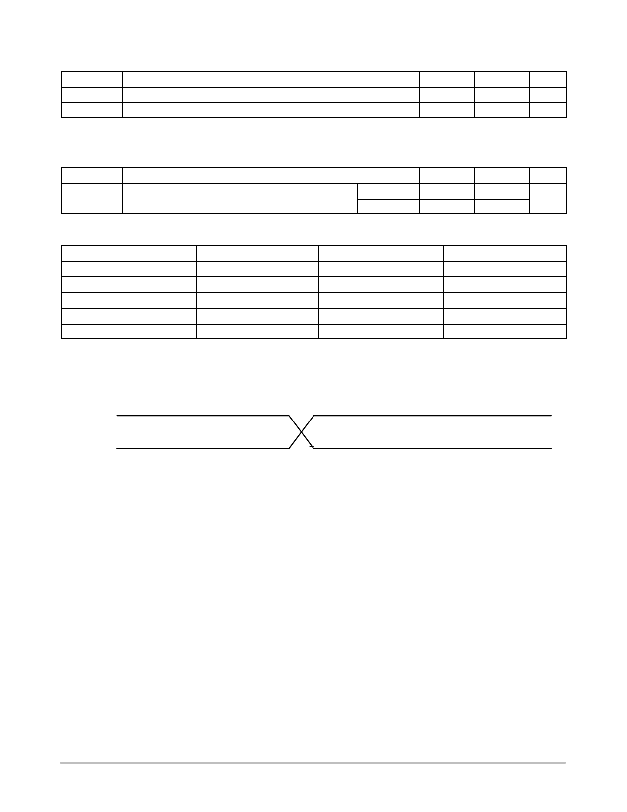
VCC x 0.8
VCC x 0.2
INPUT PULSE LEVELS
VCC x 0.7
VCC x 0.3
REFERENCE POINTS
Figure 2. AC Testing Input/Output Waveform (Notes 11, 12 and 13) (CL = 100 pF)
11. Input Rise and Fall Times (10% to 90%) < 10 ns.
12. Input Pulse Levels = VCC x 0.2 and VCC x 0.8.
13. Input and Output Timing Reference = VCC x 0.3 and VCC x 0.7.
http://onsemi.com
4
Share Link: 