CS8161YT5 查看數據表(PDF) - ON Semiconductor
零件编号
产品描述 (功能)
生产厂家
CS8161YT5 Datasheet PDF : 11 Pages
| |||
CS8161
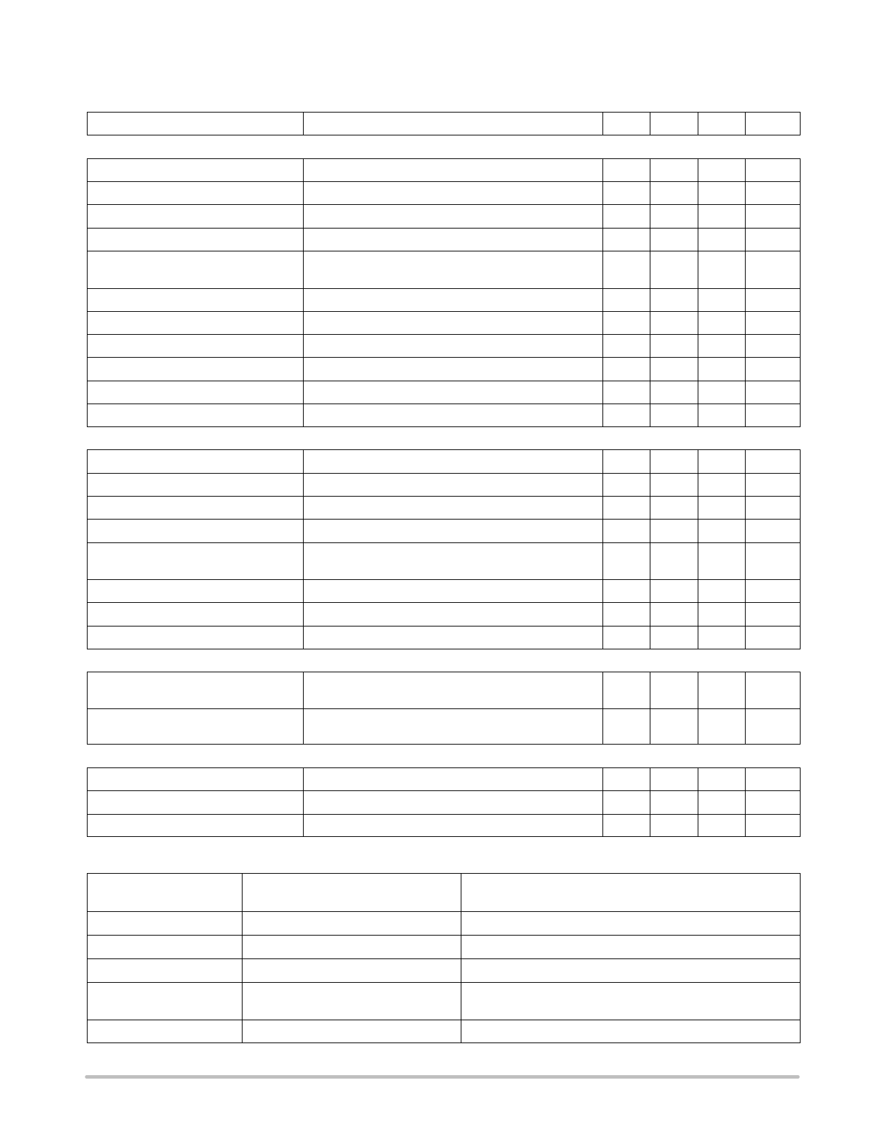
ELECTRICAL CHARACTERISTICS for VOUT: (6.0 V ≤ VIN ≤ 26 V; IOUT1 = 5.0 mA; IOUT2 = 5.0 mA;
−40°C ≤ TJ ≤ +150°C; −40°C ≤ TA ≤ +125°C; unless otherwise specified.)
Characteristic
Test Conditions
Min Typ Max
PRIMARY OUTPUT STAGE (VOUT1)
Output Voltage, VOUT1
Dropout Voltage
Line Regulation
Load Regulation
Quiescent Current
Ripple Rejection
Current Limit
13 V ≤ VIN ≤ 26 V, IOUT1 ≤ 400 mA
IOUT1 = 400 mA
13 V ≤ VIN ≤ 20 V, 5.0 mA ≤ IOUT < 400 mA
5.0 mA ≤ IOUT1 ≤ 400 mA, VIN = 14 V
IOUT1 ≤ 100 mA, No Load on VOUT2
IOUT1 ≤ 400 mA, No Load on VOUT2
f = 120 Hz, IOUT = 300 mA, VIN = 15.0 VDC, 2.0 VRMS
−
11.4 12.0 12.6
−
0.35 0.6
−
−
80
−
−
80
−
8.0
12
−
50
75
42
−
−
0.40
−
1.0
Reverse Polarity Input Voltage, DC
VOUT1 ≥ −0.6 V, 10 W Load
−
Reverse Polarity Input Voltage, Transient 1.0% Duty Cycle, t = 100 ms, VOUT ≥ −6.0 V, 10 W Load −
Overvoltage Shutdown
−
28
−30 −18
−80 −50
34
45
Short Circuit Current
−
−
−
700
SECONDARY OUTPUT (VOUT2)
Output Voltage, (VOUT2)
Dropout Voltage
Line Regulation
Load Regulation
Quiescent Current
6.0 V ≤ VIN ≤ 26 V, IOUT2 ≤ 200 mA
IOUT2 ≤ 200 mA
6.0 V ≤ VIN ≤ 26 V, 1.0 mA ≤ IOUT ≤ 200 mA
1.0 mA ≤ IOUT2 ≤ 200 mA; VIN =14 V
IOUT2 = 50 mA
IOUT2 = 200 mA
4.90
−
5.10
−
0.35 0.60
−
−
50
−
−
50
−
5.0
10
−
20
35
Ripple Rejection
Current Limit
f = 120 Hz; IOUT = 10 mA, VIN = 15 V, 2.0 VRMS
−
42
−
−
200
−
600
Short Circuit Current
−
−
−
400
ENABLE FUNCTION (ENABLE)
Input ENABLE Threshold
Input ENABLE Current
OTHER FEATURES
VOUT1 Off
VOUT1 On
VENABLE = 5.5 V
VENABLE < 0.8 V
−
1.30 0.80
2.00 1.30
−
80
−
500
−10
−
10
Sleep Mode
Thermal Shutdown
VENABLE < 0.4 V
−
−
0.2
50
150
−
210
Quiescent Current in Dropout
IOUT1 = 100 mA, IOUT2 = 50 mA
−
−
60
Unit
V
V
mV
mV
mA
mA
dB
A
V
V
V
mA
V
V
mV
mV
mA
mA
dB
mA
mA
V
V
mA
mA
mA
°C
mA
PACKAGE PIN DESCRIPTION
PACKAGE LEAD #
5 Lead TO−220
1
2
3
4
5
LEAD SYMBOL
VIN
VOUT1
GND
ENABLE
VOUT2
FUNCTION
Supply voltage, usually direct from battery.
Regulated output 12 V, 400 mA (typ).
Ground connection.
CMOS compatible input lead; switches outputs on and off.
When ENABLE is high VOUT1 and VOUT2 are active.
Regulated output 5.0 V, 200 mA (typ).
http://onsemi.com
3
Share Link: 