CS8161YT5 查看數據表(PDF) - ON Semiconductor
零件编号
产品描述 (功能)
生产厂家
CS8161YT5 Datasheet PDF : 11 Pages
| |||
CS8161
The values for the output capacitors C2 and C3 shown in
the test and applications circuit should work for most
applications, however it is not necessarily the best solution.
To determine acceptable values for C2 and C3 for a
particular application, start with tantalum capacitors of the
recommended value on each output and work towards less
expensive alternative parts for each output in turn.
Step 1: Place the completed circuit with a tantalum
capacitor of the recommended value in an environmental
chamber at the lowest specified operating temperature and
monitor the outputs on the oscilloscope. A decade box
connected in series with the capacitor C2 will simulate the
higher ESR of an aluminum capacitor.(Leave the decade
box outside the chamber, the small resistance added by the
longer leads is negligible)
Step 2: With the input voltage at its maximum value,
increase the load current slowly from zero to full load while
observing the output for any oscillations. If no oscillations
are observed, the capacitor is large enough to ensure a stable
design under steady state conditions.
Step 3: Increase the ESR of the capacitor from zero using the
decade box and vary the load current until oscillations
appear. Record the values of load current and ESR that cause
the greatest oscillation. This represents the worst case load
conditions for the regulator at low temperature.
Step 4: Maintain the worst case load conditions set in step
3 and vary the input voltage until the oscillations increase.
This point represents the worst case input voltage
conditions.
Step 5: If the capacitor C2 is adequate, repeat steps 3 and 4
with the next smaller valued capacitor. (A smaller capacitor
will usually cost less and occupy less board space.) If the
capacitor oscillates within the range of expected operating
conditions, repeat steps 3 and 4 with the next larger standard
capacitor value.
Step 6: Test the load transient response by switching in
various loads at several frequencies to simulate its real work
environment. Vary the ESR to reduce ringing.
Step 7: Raise the temperature to the highest specified
operating temperature. Vary the load current as instructed in
step 5 to test for any oscillations.
Once the minimum capacitor value with the maximum
ESR is found, a safety factor should be added to allow for the
tolerance of the capacitor and any variations in regulator
performance. Most good quality aluminum electrolytic
capacitors have a tolerance of ±20% so the minimum value
found should be increased by at least 50% to allow for this
tolerance plus the variation which will occur at low
temperatures. The ESR of the capacitors should be less than
50% of the maximum allowable ESR found in step 3 above.
Once the value for C2 is determined, repeat the steps to
determine the appropriate value for C3.
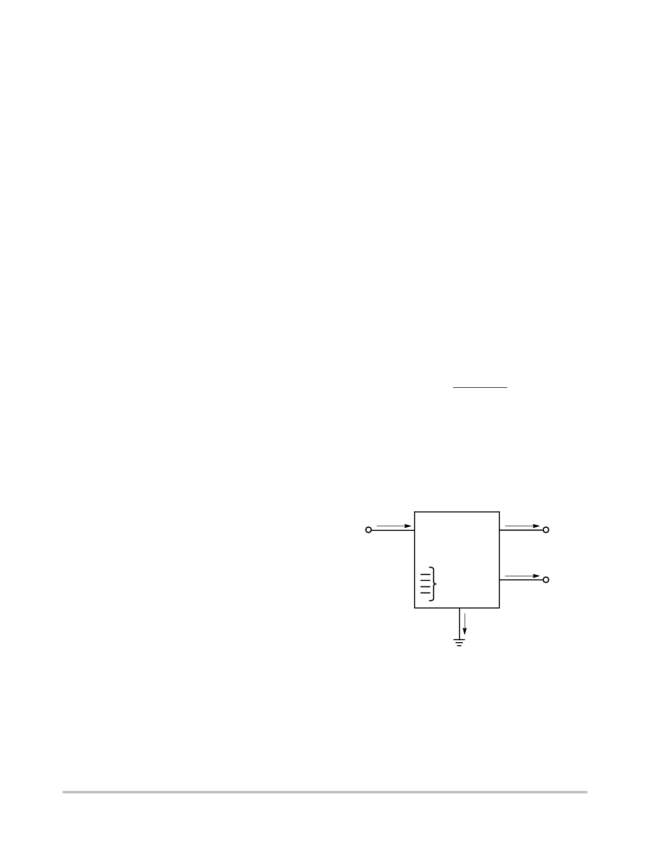
Calculating Power Dissipation in a
Dual Output Linear Regulator
The maximum power dissipation for a dual output
regulator (Figure 19) is
PD(max) + NJVIN(max) * VOUT1(min)NjIOUT1(max) )
NJVIN(max) * VOUT2(min)NjIOUT2(max) ) VIN(max)IQ (1)
where:
VIN(max) is the maximum input voltage,
VOUT1(min) is the minimum output voltage from VOUT1,
VOUT2(min) is the minimum output voltage from VOUT2,
IOUT1(max) is the maximum output current, for the
application,
IOUT2(max) is the maximum output current, for the
application, and
IQ is the quiescent current the regulator consumes at
IOUT(max).
Once the value of PD(max) is known, the maximum
permissible value of RqJA can be calculated:
RqJA
+
150°C *
PD
TA
(2)
The value of RqJA can be compared with those in the
package section of the data sheet. Those packages with
RqJA’s less than the calculated value in equation 2 will keep
the die temperature below 150°C.
In some cases, none of the packages will be sufficient to
dissipate the heat generated by the IC, and an external
heatsink will be required.
IIN
VIN
Smart
Regulator
IOUT1
VOUT1
Control
Features
IOUT2
VOUT2
IQ
Figure 19. Dual Output Regulator With Key
Performance Parameters Labeled.
http://onsemi.com
8
Share Link: 