DLG4137 وں¥çœ‹و•¸و“ڑè،¨ï¼ˆPDF) - OSRAM GmbH
零ن»¶ç¼–هڈ·
ن؛§ه“پوڈڈè؟° (هٹں能)
ç”ںن؛§هژ‚ه®¶
DLG4137 Datasheet PDF : 4 Pages
| |||
If small wire cables are used, good engineering practice is to
calculate the wire resistance of the ground and the +5 volt
wires. More than 0.2 volt drop (at 100 ma per digit) should be
avoided, since this loss is in addition to any inaccuracies or load
regulation of the power supply.
The 5 volt power supply for the DLO4135/DLG4137 should be
the same one supplying the VCC to all logic devices. If a separate
power supply must be used, then local buffers should be used
on all the inputs. These buffers should be powered from the dis-
play power supply. This precaution is to avoid line transients or
any logic signals to be higher than VCC during power up.
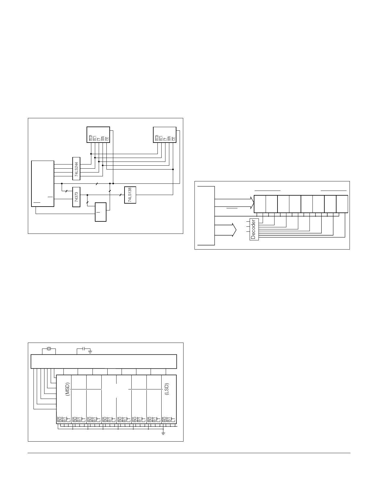
Figure 5. Block diagram of the Intel 8031 controller
Dأک
D7
xxxxx
P3.0
P3.1
P3.2
P3.6
8031 Pأک
ALE
PSEN
BUFFER
8
8
LATCH
8
A0-A7
OE
8
3
DECODER
EPROM
27xx
Subroutine to Load an 8-digit Display using the DLO4135/
DLG4137
INIT ORL
ORL
MOV
MOV
MOV
START: INC
DATA: MOV
OUTL
MOV
RR
MOV
WRITE: OUTL
MOV
OUTL
DJNZ
RET
P1,#0FFH
P2,#00H
R1,#OFH
R2,#0FEH
R3,#08H
R1
A,@R1
P2,A
A,R2
A
R2,A
P1,A
A,#OFFH
P1,A
R3,START
; DATA IN RAM 10H-17H
(MSD-LSD)
; PORT 1 ALL HIGH (WRITE)
; PORT 2 ALL LOW (DATA)
; RAM ADDRESS—1
; WRITE PULSE
; COUNTER
; INCREMENT RAM POINTER
; FETCH DATA FROM RAM
; LOAD PORT 2
; RECALL WRITE
; SHIFT A TO NEXT WRITE
; SAVE WRITE
; SEND WRITE PULSE
; WAIT
; RESET WRITE PULSE
; LOAD COMPLETE?
; RETURN TO MAIN PROGRAM
Figure 7. Block diagram for 8-digit DLO4135/DLG4137
Eight DLX413X
8080
or
8085
Data
I/OW
System
A0
Address
A1
A2
Interfacing
For an eight digit display using the DLO4135/DLG4137, inter-
facing to a single chip microprocessor such as the 8748, is easy
and straight forward. One approach may be to dedicate one
port for the seven data signals and another 8-bit port for the
write signals. The schematic is shown in Figure 6.
I/O or Memory Mapped System
For a memory mapped system using a processor such as the
8080 or 8085, the interfacing is also straight-forward. Each dis-
play is treated as a memory location with its own address, like
another I/O or RAM location. See Figure 7.
Figure 6. DLO4135/DLG4137 with 8748
P2
8748
P1
6543210 7
6
5
4
3
2
1
0
D0
D1
D2
DLO 4135
D3
DLG 4137
D4
D5
D6
+
Routine for an 8-Digit Display using the DLO4135/DLG4137
and 8085 or 8080 Microprocessor
DADD EQU 0A000H
DPAD EQU 0C000H
LEN EQU 08H
ORG 100H
DISP: LXI H,DADD
LXI D,DPAD
MVI B,LEN
DISP1: MOV A,M
XCHG
MOV M,A
XCHG
INX D
INX H
DCR B
JNZ DISP1
RET
; DATA TO BE DISPLAYED IS IN
; A0 (LSD) THRU A7 (MSD)
;
; DISPLAY ADDRESS C00X
; LSD IS RIGHT MOST DIGIT
;
; DOES NOT SAVE REG A,B,H,L,D,E
;
; DATA ADDRESS LOCATION
; DISPLAY ADDRESS
LOCATION
; DISPLAY LENGTH
;
;
; LOAD DATA ADDRESS
; LOAD DISPLAY ADDRESS
; LOAD DISPLAY LENGTH
; GET DATA
; XCHG H/L & D/E
; LOAD DISPLAY FROM REG A
; RESTORE H/L & D/E
; INCREMENT DISPLAY ADDRESS
; INCREMENT DATA ADDRESS
; DECREMENT LENGTH COUNTER
; END OF DISPLAY?
; RETURN TO MAIN PROGRAM
 2000 Inï¬پneon Technologies Corp. • Optoelectronics Division • San Jose, CA
www.inï¬پneon.com/opto • 1-888-Inï¬پneon (1-888-463-4636)
OSRAM Opto Semiconductors GmbH & Co. OHG • Regensburg, Germany
www.osram-os.com • +49-941-202-7178
3
Appnote 28
May 31, 2000-13
Share Link: 