SFC05-4TM 查看數據表(PDF) - Semtech Corporation
零件编号
产品描述 (功能)
生产厂家
SFC05-4TM Datasheet PDF : 7 Pages
| |||
PROTECTION PRODUCTS
Applications Information (Continued)
Printed Circuit Board Finish
A uniform board finish is critical for good assembly
yield. Two finishes that provide uniform surface coat-
ings are immersion nickel gold and organic surface
protectant (OSP). A non-uniform finish such as hot air
solder leveling (HASL) can lead to mounting problems
and should be avoided.
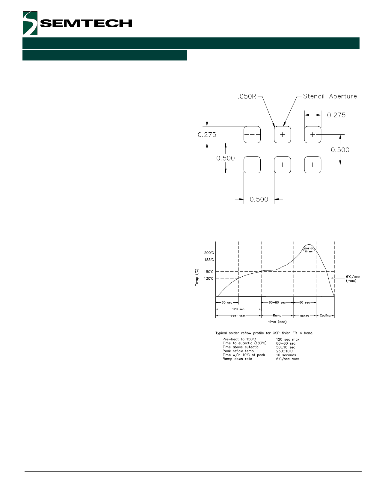
Stencil Design
A properly designed stencil is key to achieving ad-
equate solder volume without compromising assembly
yields. A 0.100mm thick, laser cut, electro-polished
stencil with 0.275mm square apertures and rounded
corners is recommended.
Reflow Profile
The flip chip TVS can be assembled using standard
SMT reflow processes. As with any component, ther-
mal profiles at specific board locations can vary & must
be determined by the manufacturer. The flip chip TVS
peak reflow temperature is 230 ± 10 °C, but the
device can withstand up to 260 °C peak reflow tem-
perature. Time above eutectic temperature (183 °C)
should be 50 ± 10 seconds. During reflow, the compo-
nent self-aligns itself on the pad.
Circuit Board Layout Recommendations for Suppres-
sion of ESD
Good circuit board layout is critical for the suppression
of ESD induced transients. The following guidelines are
recommended:
l Place the TVS near the input terminals or connec-
tors to restrict transient coupling.
l Minimize the path length between the TVS and the
protected line.
l Minimize all conductive loops including power and
ground loops.
l The ESD transient return path to ground should be
kept as short as possible.
l Never run critical signals near board edges.
l Use ground planes whenever possible.
ã 2000 Semtech Corp.
5
SFC05-4
PRELIMINARY
Stencil Design
Reflow Profile
www.semtech.com
Share Link: 