FM25C160B(2014) жҹҘзңӢж•ёж“ҡиЎЁпјҲPDFпјү - Cypress Semiconductor
йӣ¶д»¶зј–еҸ·
дә§е“ҒжҸҸиҝ° (еҠҹиғҪ)
з”ҹдә§еҺӮ家
FM25C160B Datasheet PDF : 20 Pages
| |||
FM25C160B
Data Transmission (SI/SO)
The SPI data bus consists of two lines, SI and SO, for serial data
communication. SI is also referred to as Master Out Slave In
(MOSI) and SO is referred to as Master In Slave Out (MISO). The
master issues instructions to the slave through the SI pin, while
the slave responds through the SO pin. Multiple slave devices
may share the SI and SO lines as described earlier.
The FM25C160B has two separate pins for SI and SO, which can
be connected with the master as shown in Figure 2.
For a microcontroller that has no dedicated SPI bus, a
general-purpose port may be used. To reduce hardware
resources on the controller, it is possible to connect the two data
pins (SI, SO) together and tie off (HIGH) the HOLD and WP pins.
Figure 3 shows such a configuration, which uses only three pins.
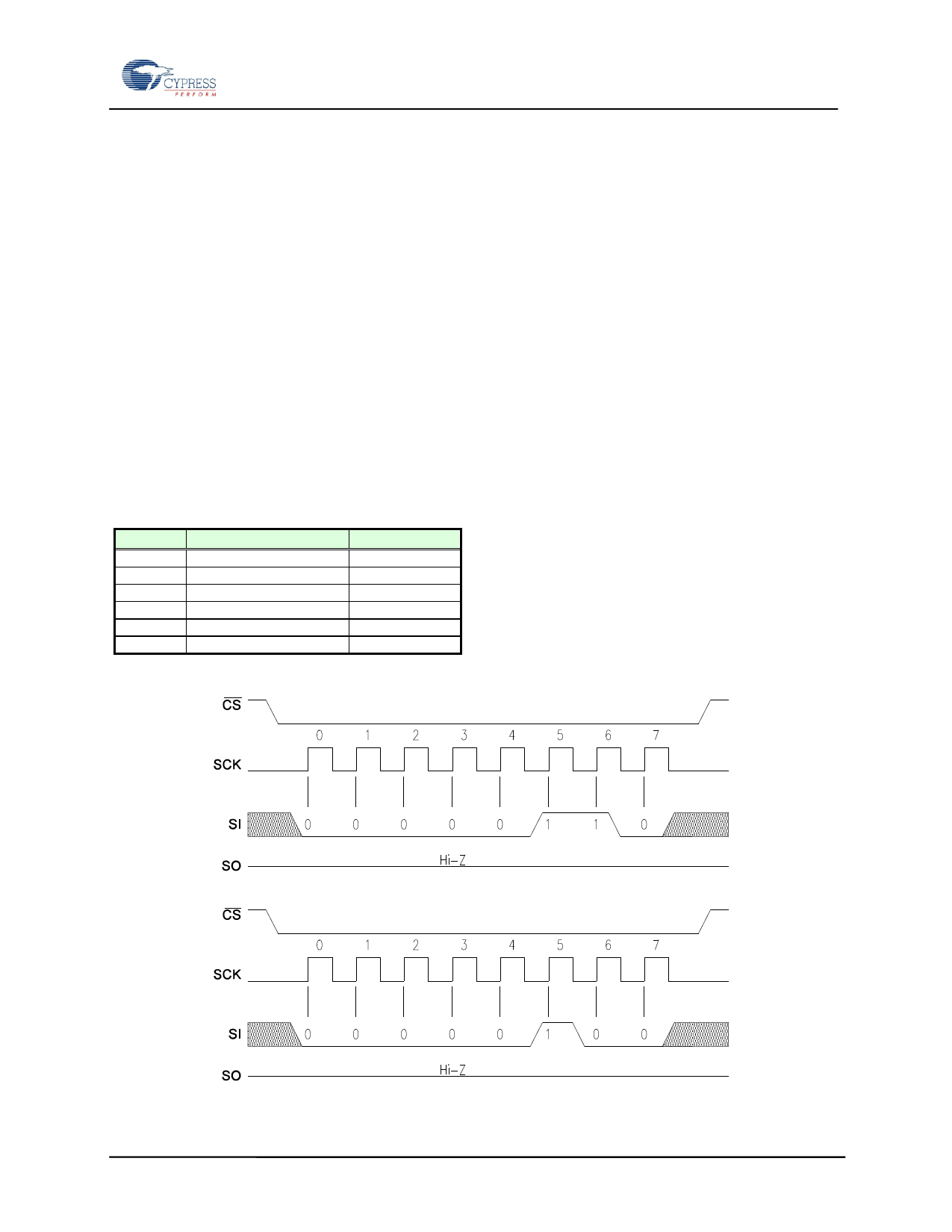
Most Significant Bit (MSB)
The SPI protocol requires that the first bit to be transmitted is the
Most Significant Bit (MSB). This is valid for both address and
data transmission.
five bits which are fed in are ignored by the device. Although
these three bits are вҖҳdonвҖҷt careвҖҷ, Cypress recommends that these
bits be set to 0s to enable seamless transition to higher memory
densities.
Serial Opcode
After the slave device is selected with CS going LOW, the first
byte received is treated as the opcode for the intended operation.
FM25C160B uses the standard opcodes for memory accesses.
Invalid Opcode
If an invalid opcode is received, the opcode is ignored and the
device ignores any additional serial data on the SI pin until the
next falling edge of CS, and the SO pin remains tristated.
Status Register
FM25C160B has an 8-bit Status Register. The bits in the Status
Register are used to configure the device. These bits are
described in Table 3 on page 7.
The 16-Kbit serial F-RAM requires a 2-byte address for any read
or write operation. Because the address is only 11 bits, the first
Figure 2. System Configuration with SPI port
SCK
MOSI
MISO
SPI
Microcontroller
CS1
HOLD1
WP1
CS2
HOLD2
WP2
SCK SI SO
FM25C160B
CS HOLD WP
SCK SI SO
FM25C160B
CS HOLD WP
Figure 3. System Configuration without SPI port
P1.0
P1.1
Microcontroller
SCK SI SO
FM25C160B
CS HOLD WP
P1.2
Document Number: 001-86150 Rev. *A
Page 5 of 20
Share Link: 