FP2189-PCB1900S 查看數據表(PDF) - Unspecified
零件编号
产品描述 (功能)
生产厂家
FP2189-PCB1900S Datasheet PDF : 6 Pages
| |||
FP2189
1 Watt HFET
The Communications Edge TM
Preliminary Product Information
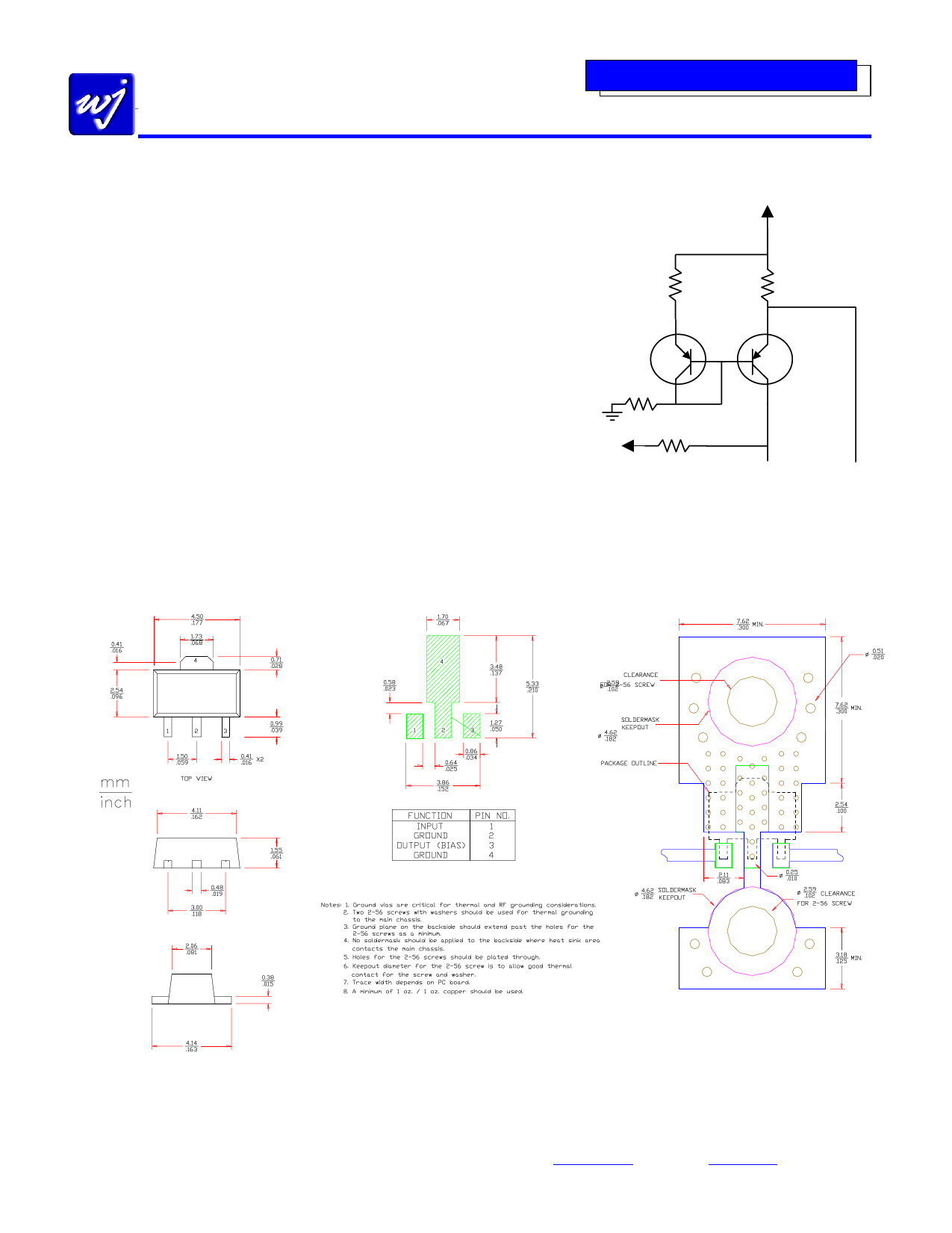
Application Note
Special attention should be taken to properly bias the FP2189. Power supply sequencing
is required to prevent the device from operating at 100% Idss for a prolonged period of
time and possibly causing damage to the device. It is recommended that for the safest
operation, the negative supply be “first on and last off.” With a negative gate voltage
present, the drain voltage can then be applied to the device. The gate voltage can then
be adjusted to have the device be used at the proper quiescent bias condition.
An optional temperature-compensation active-bias circuit is recommended for use with
the application circuit, which requires two standard voltage supplies +8V and -4V, and
is set for an optimal drain bias of +8V @ 250 mA. The circuit schematic, shown on the
right, uses dual PNP transistors to provide a constant drain current into the FP2189 and
also eliminates the effects of pinchoff variation. Temperature compensation is achieved
by tracking the voltage variation with the temperature of the emitter-to-base junction of
the PNP transistors. Thus the transistor emitter voltage adjusts the voltage incident at
the gate of the FP2189 so that the device draws a constant current, regardless of the
temperature. Two fixed voltage supplies are needed for operation. A Rohm dual
transistor, UMT1N, and a dual-chip resistor (8.2 kΩ) are recommended to minimize
board space and help decrease the current variability through R4 with the components
being matched to one another. The active-bias circuit can directly be attached to the
voltage supply ports in the circuit diagram as shown above (Vdd and Vgg).
Vdd = +8 V
R3
220 Ω
4
25
R5
8.2 kΩ
3
R6
Vgg = -4 V 8.2 kΩ
R4
1Ω
1%
0805
1
UMT1N
6
Connected to Vgg
on App Circuit
Connected to Vdd
on App Circuit
Outline Drawing
Land Pattern
Mounting Configuration
This document contains information on a new product.
Specifications and information are subject to change without notice
WJ Communications, Inc • Phone 1-800-WJ1-4401 • FAX: 408-577-6620 • e-mail: sales@wj.com • Web site: www.wj.com
May 2002
Share Link: 