LTC1232(RevA) 查看數據表(PDF) - Linear Technology
零件编号
产品描述 (功能)
生产厂家
LTC1232 Datasheet PDF : 8 Pages
| |||
LTC1232
PI FU CTIO S
RST: Open Drain Logic Output for µP Reset Control.
The LTC1232 provides three ways to generate µP reset.
First, when VCC falls below VCC trip point (4.75V with
TOL = GND and 4.5V with TOL = VCC), RST goes active low.
After VCC returns to 5V, the reset pulse generator forces
RST to remain active low for a minimum of 250ms.
Second, when the watchdog timer is not serviced prior to
a selected time-out period, the reset pulse generator also
forces RST to active low for a minimum of 250ms and
repeats for every time-out period. Third and the last, when
the PB RST pin stays active low for a minimum of 40ms,
RST becomes active low. The RST output will remain
active low for a minimum of 250ms from the moment the
push-button reset input is released from logic low level.
RST: RST is an Active High Logic Output. It is the inverse
of RST.
ST: Logic Input to Reset the Watchdog Timer. Driving ST
either high or low longer than the time-out period set by
the TD input, forces the reset outputs to active states for
a minimum of 250ms. The timer resets itself and begins to
time-out again with each high to low transition on the ST
input (see Figure 2).
APPLICATIO S I FOR ATIO
Power Monitoring
The LTC1232 uses a bandgap voltage reference and a
precision voltage comparator, C1, to monitor the 5V
supply input on VCC (see Block Diagram). When VCC falls
below the VCC trip point (4.62V typical with
TOL = GND and 4.37V typical with TOL VCC), the reset
outputs are forced to active states. The VCC trip point
accounts for a 5% or 10% variation on VCC, so the reset
outputs become active when VCC falls below the VCC trip
point. On power-up, the reset signals are held in active
states for a minimum of 250ms after the VCC trip point is
reached to allow the power supply and microprocessor
to stabilize. On power-down, the RST signal remains
active low even with VCC as low as 1V. This capability helps
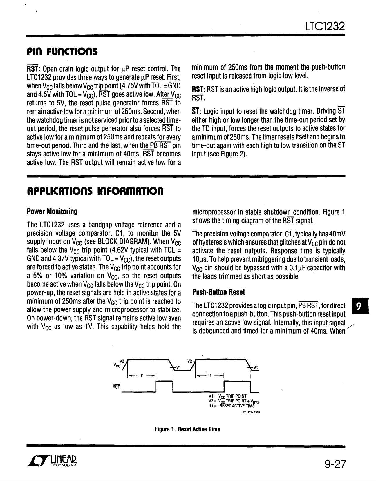
hold the microprocessor in stable shutdown condition.
Figure 1 shows the timing diagram of the RST signal.
The precision voltage comparator, C1, typically has 40mV
of hysteresis which ensures that glitches at VCC pin do not
activate the reset outputs. Response time is typically 10µs.
To help prevent mitriggering due to transient loads, VCC
pin should be bypassed with a 0.1µF capacitor with the
leads trimmed as short as possible.
Push-Button Reset
The LTC1232 provides a logic input pin, PB RST, for direct
connection to a push-button. This push-button reset input
requires an active low signal. Internally, this input signal is
debounced and timed for a minimum of 40ms. When this
6
V2
VCC
RST
V2
V1
V1
t1
t1
V1 = VCC TRIP POINT
V2 = VCC TRIP POINT + VHYS
t1 = RESET ACTIVE TIME
LTC1232 • TA03
Figure 1. Reset Active Time
sn1232 1232fas
Share Link: 