LTC1232(RevA) 查看數據表(PDF) - Linear Technology
零件编号
产品描述 (功能)
生产厂家
LTC1232 Datasheet PDF : 8 Pages
| |||
LTC1232
APPLICATIO S I FOR ATIO
condition is satisfied, the reset pulse generator forces the
reset outputs to active states. The reset signals will remain
active for a minimum of 250ms from the moment the
push-button reset input is released from logic low level
(see Timing Diagram).
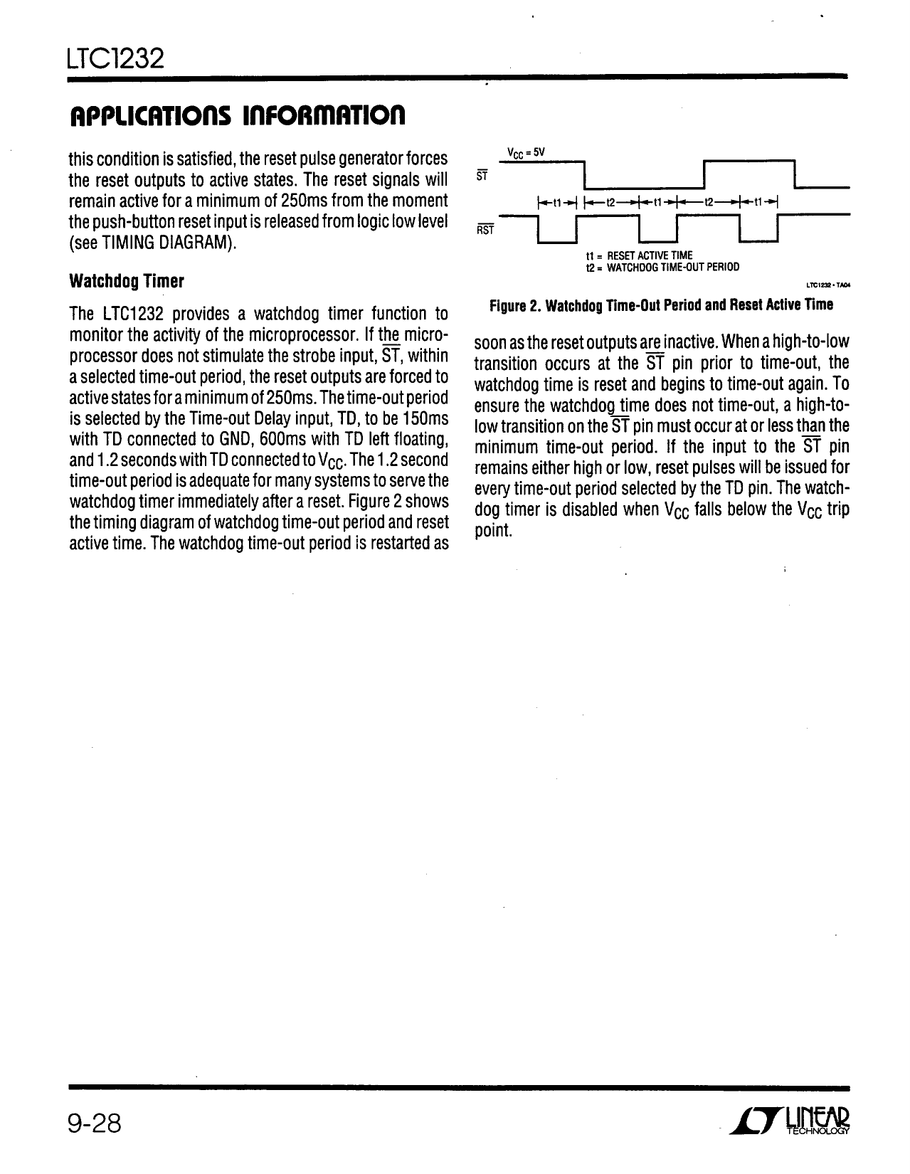
Watchdog Timer
The LTC1232 provides a watchdog timer function to
monitor the activity of the microprocessor. If the micro-
processor does not stimulate the strobe input, ST, within
a selected time-out period, the reset outputs are forced to
active states for a minimum of 250ms. The time-out period
is selected by the Time-Out Delay input, TD, to be 150ms
with TD connected to GND, 600ms with TD left floating,
and 1.2 seconds with TD connected to VCC. The 1.2 second
time-out period is adequate for many systems to serve the
watchdog timer immediately after a reset. Figure 2 shows
the timing diagram of watchdog time-out period and reset
active time. The watchdog time-out period is restarted as
VCC = 5V
ST
t1
t2
t1
t2
t1
RST
t1 = RESET ACTIVE TIME
t2 = WATCHDOG TIME-OUT PERIOD
LTC1232 • TA04
Figure 2. Watchdog Time-Out Period and Reset Active Time
soon as the reset outputs are inactive. When a high-to-low
transition occurs at the ST pin prior to time-out, the
watchdog time is reset and begins to time-out again. To
ensure the watchdog time does not time-out, a high-to low
transition on the ST pin must occur at or less than the
minimum time-out period. If the input to the ST pin
remains either high or low, reset pulses will be issued for
every time-out period selected by the TD pin. The watch-
dog timer is disabled when VCC falls below the VCC trip
point.
PACKAGE DESCRIPTIO
N8 Package
8-Lead PDIP (Narrow .300 Inch)
(Reference LTC DWG # 05-08-1510)
.400*
(10.160)
MAX
8
7
6
5
.255 ± .015*
(6.477 ± 0.381)
.300 – .325
(7.620 – 8.255)
12
.045 – .065
(1.143 – 1.651)
34
.130 ± .005
(3.302 ± 0.127)
.009 – .015
(0.229 – 0.381)
.065
(1.651)
TYP
+.035
.325 –.015
( ) 8.255
+0.889
–0.381
.100
(2.54)
BSC
NOTE:
1. DIMENSIONS
ARE
INCHES
MILLIMETERS
*THESE DIMENSIONS DO NOT INCLUDE MOLD FLASH OR PROTRUSIONS.
MOLD FLASH OR PROTRUSIONS SHALL NOT EXCEED .010 INCH (0.254mm)
.125
(3.175)
MIN
.018 ± .003
(0.457 ± 0.076)
.020
(0.508)
MIN
N8 0502
Information furnished by Linear Technology Corporation is believed to be accurate and reliable.
However, no responsibility is assumed for its use. Linear Technology Corporation makes no represen-
tation that the interconnection of its circuits as described herein will not infringe on existing patent rights.
sn1232 1232fas
7
Share Link: 