M66004SP وں¥çœ‹و•¸و“ڑè،¨ï¼ˆPDF) - Mitsumi
零ن»¶ç¼–هڈ·
ن؛§ه“پوڈڈè؟° (هٹں能)
ç”ںن؛§هژ‚ه®¶
M66004SP Datasheet PDF : 14 Pages
| |||
MITSUBISHI 〈DIGITAL ASSPâŒھ
M66004SP/FP
16-DIGIT 5X7-SEGMENT VFD CONTROLLER
PIN DESCRIPTIONS
Symbol Pin name
Function
RESET Reset input This pin is used to initialize the internal state of the M66004.
CS
Chip select In “L†state, communication with the MCU is possible.
input
In “H†state, any instruction from the MCU is neglected.
SCK
Shift clock
input
At the rising edge from “L†to “Hâ€, input data is shifted.
SDATA
Serial data
input
Character code or command data to display is input from MSB.
XIN,
XOUT
Clock input
Clock output
This pin is used to connect a resistor and a capacitor externally to set oscillation frequency. (maximum
oscillation frequency fosc(max)=1MHz) An external clock can be also connected. In this case, an external
clock is connected to pin XIN, and pin XOUT is set to be in open state.
DIG00~
DIG15
Digit output
These pins are used to connect to digit pins of VFD. Pins from DIG00 to DIG15 correspond to digits of VFD
from the first digit to the 16th digit.
SEG00~ Segment
SEG35 output
These pins are used to connect to segment pins of VFD. Pins from SEG00 to SEG35 correspond to segment
pins of VFD as shown in the table below.
P0, P1
Output port (static operation)
VCC1
Positive power supply for internal logic
VCC2
Positive power supply for high-pressure-resistant output port
VSS
GND
VP
Negative power supply for VFD drive
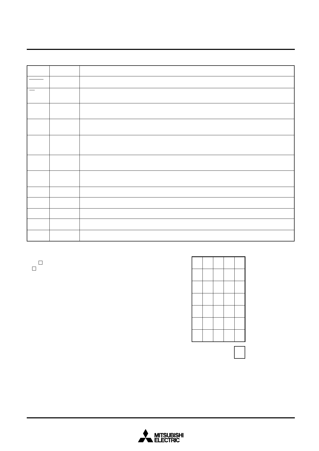
(Connection of segment output pins)
Each in the table shows one-dot segment and each figure
in shows the output segment pin number (from 00 to 35) to
connect.
00 01 02 03 04
05 06 07 08 09
10 11 12 13 14
15 16 17 18 19
20 21 22 23 24
25 26 27 28 29
30 31 32 33 34
35
3
Share Link: 