M66010GP 查看數據表(PDF) - Renesas Electronics
零件编号
产品描述 (功能)
生产厂家
M66010GP Datasheet PDF : 5 Pages
| |||
MITSUBISHI 〈DIGITAL ASSP〉
M66010FP/GP
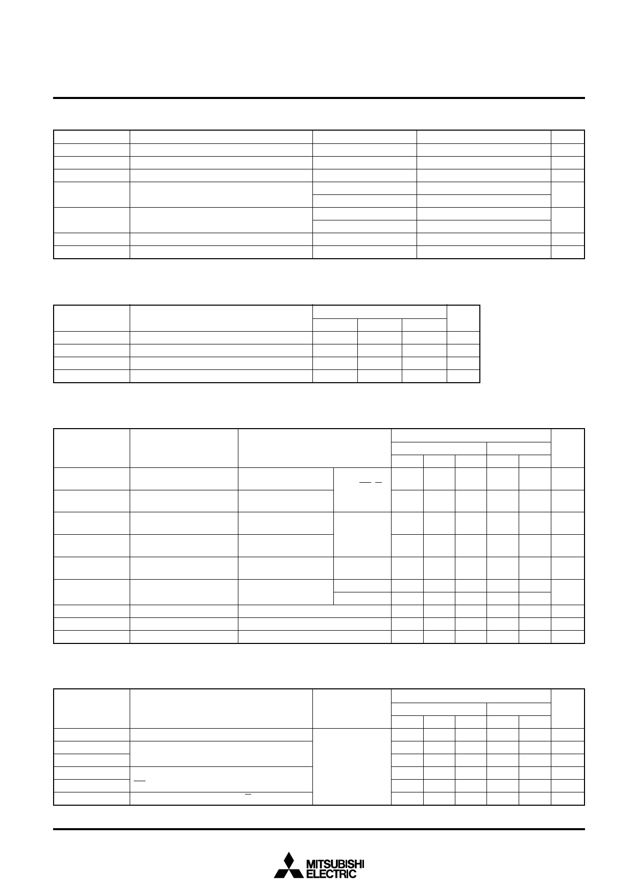
ABSOLUTE MAXIMUM RATINGS (Ta = –20 ~ 75°C unless otherwise noted)
Symbol
Parameter
Conditions
VCC
Supply voltage
VI
Input voltage
VO
Output voltage
IIK
Input protection diode current
VI<0V
VI>VCC
IOK
Output parasitic diode current
VO<0V
VO>VCC
IGND
GND current
GND
Tstg
Storage temperature
24-BIT I/O EXPANDER
Ratings
Unit
–0.5 ~ +7.0
V
–0.5 ~ VCC + 0.5
V
–0.5 ~ VCC + 0.5
V
–20
mA
20
–20
mA
20
–150
mA
–65 ~ 150
˚C
RECOMMENDED OPERATING CONDITIONS
Symbol
Parameter
VCC
Supply voltage
VI
Input voltage
VO
Output voltage
Topr
Operating temperature
Limits
Unit
Min.
Typ.
Max.
2
6
V
0
VCC
V
0
VCC
V
–20
75
°C
ELECTRICAL CHARACTERISTICS (VCC = 2 ~ 6V unless otherwise noted)
Symbol
Parameter
Test conditions
Limits
Ta=25˚C
Ta= –20~75˚C Unit
Min. Typ. Max. Min. Max.
VT+
Upper threshold voltage
VO=0.1V, VCC–0.1V
|IO|=20µA
0.35
CLK, CS, S, × VCC
0.8 0.35 0.8
× VCC × VCC × VCC
V
VT–
Lower threshold voltage
VO=0.1V, VCC–0.1V
|IO|=20µA
DI
0.2
× VCC
0.65 0.2 0.65
× VCC × VCC × VCC
V
VIH
High-level input voltage
VO=0.1V, VCC–0.1V
|IO|=20µA
0.75
× VCC
0.75
× VCC
V
VIL
Low-level input voltage
VO=0.1V, VCC–0.1V
|IO|=20µA
D1 ~ D24
0.25
× VCC
0.25
× VCC
V
VOL
VI=VT+, VT–
Open drain low-level output voltage VCC=4.5V
IOL=5mA
0.4
0.5 V
IO
Output leakage current
VI=VT+, VT–
VO=VCC
VCC=6V
VO=GND
IIH
High-level Input leakage current VI=VCC
VCC=6.0V
IIL
Low-level output leakage current VI=GND
VCC=6.0V
ICC
Static power dissipation VI=VCC, GND
VCC=6.0V
1.0
10.0 µA
–1.0
–10.0
0.1
1.0 µA
–0.1
–1.0 µA
20.0
200.0 µA
SWITCHING CHARACTERISTICS (VCC = 5V)
Symbol
Parameter
Test conditions
fmax
Input clock maximum repetitive frequency
tPLZ
“L–Z” and “Z–L” outputs propagation time
tPZL
CLK-DO
CL=50pF
tPLZ
“L–Z” and “Z–L” outputs propagation time
RL=1kΩ
(Note)
tPZL
CS-D1 to D24
tPLZ
“L–Z” outputs propagation time S=DO, D1 to D24
Limits
Ta=25˚C
Min. Typ. Max.
2.5
300
300
300
300
300
Ta= –20~75˚C
Min. Max.
1.9
400
400
400
400
400
Unit
MHz
ns
ns
ns
ns
ns
3
Share Link: 