ICM7231 查看數據表(PDF) - Intersil
零件编号
产品描述 (功能)
生产厂家
ICM7231 Datasheet PDF : 16 Pages
| |||
ICM7231, ICM7232
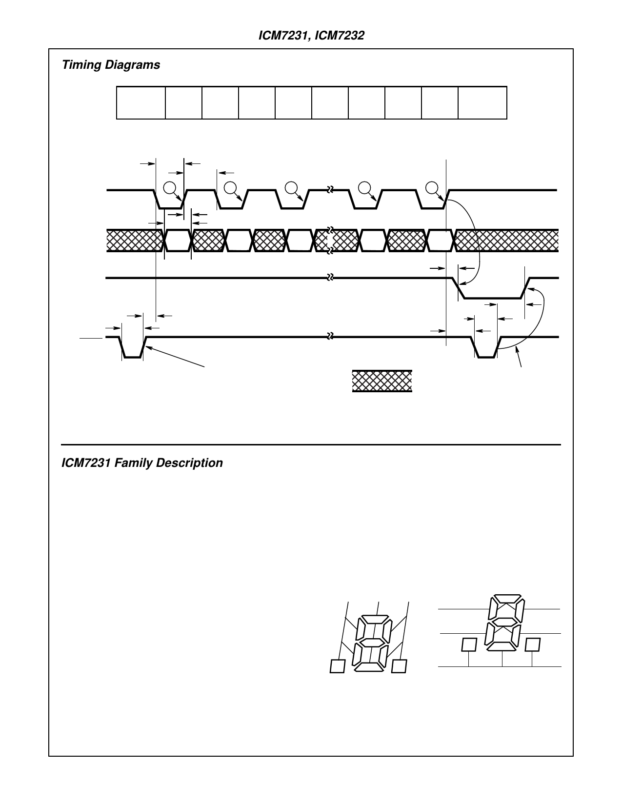
Timing Diagrams
AN1
AN2
BD0
BD1
BD2
BD3
A0
A1
A2
A3
ENTER
ENTER
FIRST
LAST
ICM7232 WRITE ORDER
DATA
CLOCK
INPUT
DATA
INPUT
tCI
tDS
1
BD0
DATA
VALID
tCI
2
tDH
BD1
DATA
VALID
3
BD2
DATA
VALID
7
A2
DATA
VALID
8
A3
DATA
VALID
DATA
ACCEPTED
OUTPUT
tWLL
tWP
WRITE
INPUT
tODI
tCWS
tODH
tWP
RESETS SHIFT REGISTER
AND INPUT CONTROL
LOGIC WHEN DATA
ACCEPTED HIGH
DO NOT CARE
DECODES AND STORES
DATA, RESETS SHIFT
REGISTER AND LOGIC
WHEN DATA ACCEPTED
IS LOW
FIGURE 3. ICM7232 INPUT TIMING DIAGRAM, LEAVING BOTH ANNUNCIATORS OFF
ICM7231 Family Description
The ICM7231 drives displays with 8 seven-segment digits with
two independent annunciators per digit, accepting six data
bits and three digit address bits from parallel inputs controlled
by a chip select input. The data bits are subdivided into four
binary code bits and two annunciator control bits.
The ICM7232 drives 10 seven-segment digits with two inde-
pendent annunciators per digit. To write into the display, six
bits of data and four bits of digit address are clocked serially
into a shift register, then decoded and written to the display.
Input levels are TTL compatible, and the DATA ACCEPTED
output on the serial input devices will drive one LSTTL load.
The intermediate voltage levels necessary to drive the dis-
play properly are generated by an on-chip resistor string,
and the output of a totally self-contained on-chip oscillator is
used to generate all display timing. All devices in this family
have been fabricated using Intersil’ MAXCMOS® process
and all inputs are protected against static discharge.
Triplexed (1/3 Multiplexed) Liquid Crystal Displays
Figure 4 shows the connection diagram for a typical
7-segment display with two annunciators such as would be
used with an ICM7231 or ICM7232 numeric display driver.
Figure 5 shows the voltage waveforms of the common lines
and one segment line, chosen for this example to be the “a,
g, d” segment line. This line intersects with BP1 to form the
“a” segment, BP2 to form the “g” segment and BP3 to form
the “d” segment. Figure 5 also shows the waveform of the “a,
g, d” segment line for four different ON/OFF combinations of
the “a”, “g” and “d” segments. Each intersection (segment or
annunciator) acts as a capacitance from segment line to
common line, shown schematically in Figure 6. Figure 7
shows the voltage across the “g” segment for the same four
combinations of ON/OFF segments used in Figure 5.
SEGMENT LINES
BP1
a
f
b
BP2
g
e
c
d
BP3
an2
an1
SEGMENT LINE CONNECTIONS
a
f
b
g
e
c
an2
d
an1
BACKPLANE CONNECTIONS
FIGURE 4. CONNECTION DIAGRAMS FOR TYPICAL
7-SEGMENT DISPLAYS
MAXCMOS® is a registered trademark of Intersil Corporation.
9-26
Share Link: 