MAX1720 查看數據表(PDF) - ON Semiconductor
零件编号
产品描述 (功能)
生产厂家
MAX1720 Datasheet PDF : 18 Pages
| |||
MAX1720
100
90
Figure 14 Test Setup
TA = 25°C
80
70
60
50
40
30
20
1.0 1.5 2.0 2.5 3.0 3.5 4.0 4.5 5.0 5.5
Vin, SUPPLY VOLTAGE (V)
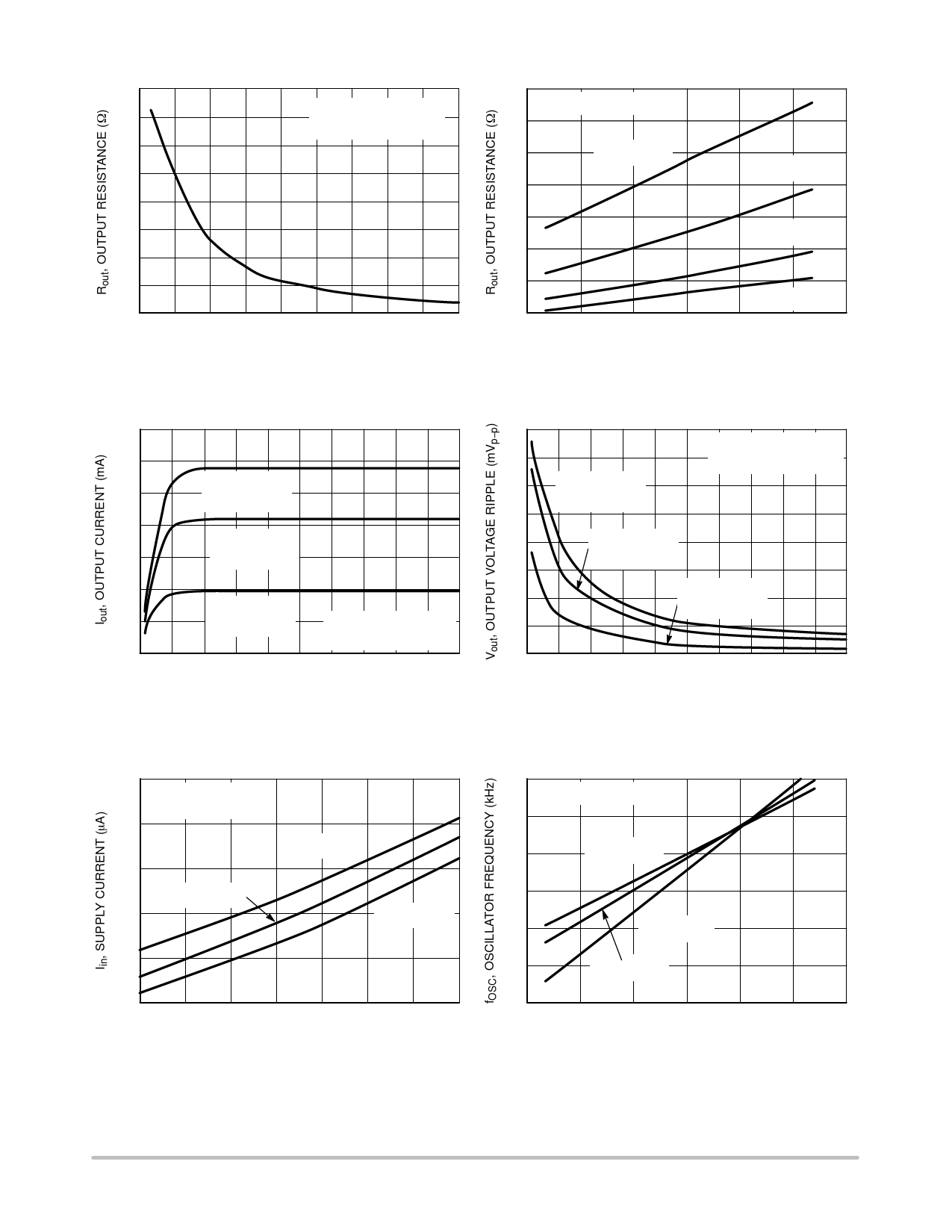
Figure 2. Output Resistance vs. Supply Voltage
90
Figure 14 Test Setup
80
70
Vin = 1.5 V
60
Vin = 2.0 V
50
Vin = 3.3 V
40
30
20
−50
Vin = 5.0 V
−25
0
25
50
75
100
TA, AMBIENT TEMPERATURE (°C)
Figure 3. Output Resistance vs. Ambient
Temperature
35
30
25
Vin = 4.75 V
Vout = −4.00 V
20
Vin = 3.15 V
15
Vout = −2.50 V
10
Vin = 1.90 V
5
Vout = −1.50 V
Figure 14 Test Setup
TA = 25°C
0
0
10
20
30
40
50
C1, C2, C3, CAPACITANCE (mF)
Figure 4. Output Current vs. Capacitance
400
350
300
250
200
150
100
50
0
0
Vin = 4.75 V
Vout = −4.00 V
Figure 14 Test Setup
TA = 25°C
Vin = 3.15 V
Vout = −2.50 V
Vin = 1.90 V
Vout = −1.50 V
10
20
30
40
50
C1, C2, C3, CAPACITANCE (mF)
Figure 5. Output Voltage Ripple vs.
Capacitance
80
Figure 14 Test Setup
RL = ∞
70
60
TA = 25°C
50
40
TA = 85°C
TA = −40°C
30
1.5 2.0 2.5 3.0 3.5 4.0 4.5 5.0
Vin, SUPPLY VOLTAGE (V)
Figure 6. Supply Current vs. Supply Voltage
13.0
Figure 14 Test Setup
12.5
12.0
Vin = 5.0 V
11.5
11.0
Vin = 1.5 V
10.5
Vin = 3.3 V
10.0
−50
−25
0
25
50
75
100
TA, AMBIENT TEMPERATURE (°C)
Figure 7. Oscillator Frequency vs. Ambient
Temperature
http://onsemi.com
3
Share Link: 