MAX1720 查看數據表(PDF) - ON Semiconductor
零件编号
产品描述 (功能)
生产厂家
MAX1720 Datasheet PDF : 18 Pages
| |||
MAX1720
The MAX1720 primary function is a voltage inverter. The device will convert 5.0 V into −5.0 V with light loads. Two capacitors
are required for the inverter to function. A third capacitor, the input bypass capacitor, may be required depending on the power
source for the inverter. The performance for this device is illustrated below.
0
−1.0
TA = 25°C
−2.0
Vin = 3.3 V
−3.0
−4.0
Vin = 5.0 V
−5.0
−6.0
0
10
20
30
40
50
Iout, OUTPUT CURRENT (mA)
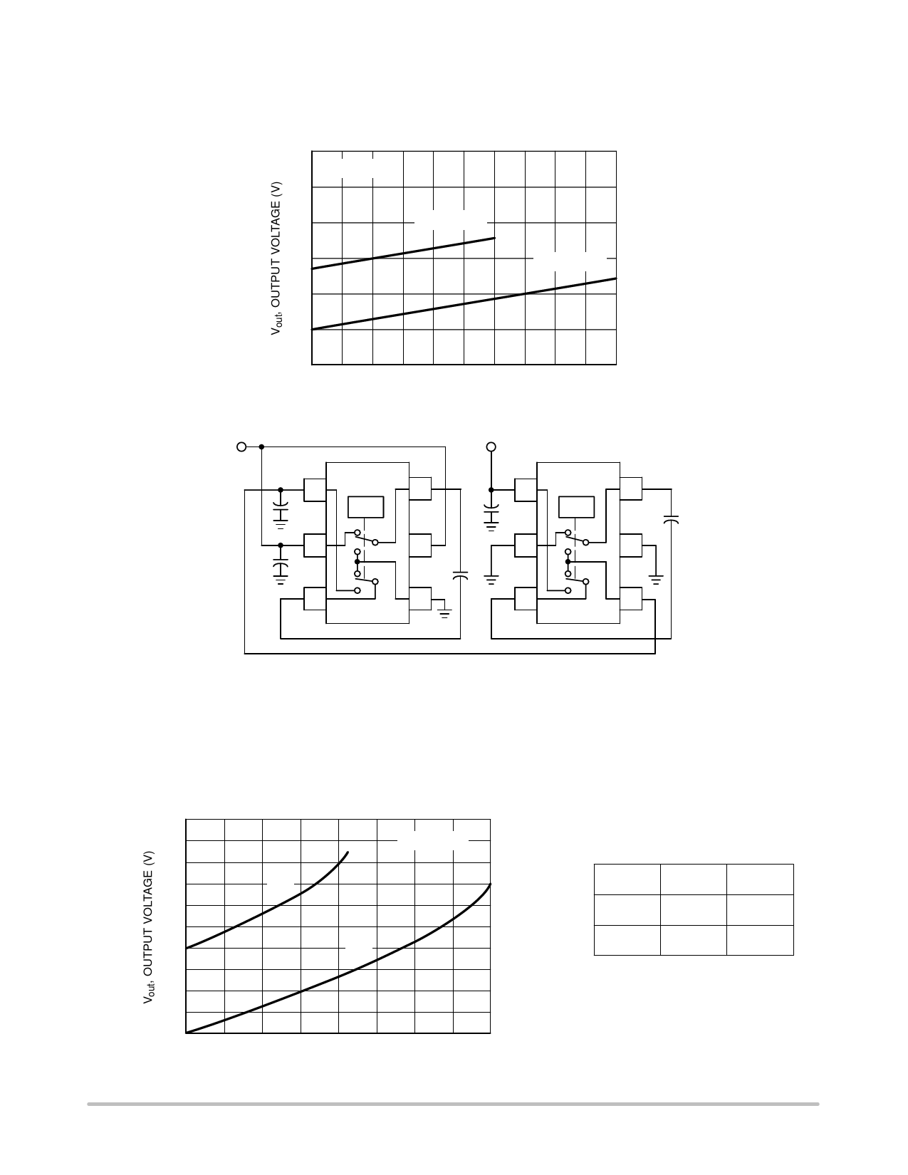
Figure 19. Inverter Load Regulation, Output Voltage vs. Output Current
Vin
−Vout
1
+
+2
OSC
3
6
5
+
4
1
+
2
OSC
6
+
5
3
4
Capacitors = 10 mF
Figure 20. Cascaded Devices for Increased Negative Output Voltage
Two or more devices can be cascaded for increased output voltage. Under light load conditions, the output voltage is
approximately equal to −Vin times the number of stages. The converter output resistance increases dramatically with each
additional stage. This is due to a reduction of input voltage to each successive stage as the converter output is loaded. Note that
the ground connection for each successive stage must connect to the negative output of the previous stage. The performance
characteristics for a converter consisting of two cascaded devices are shown below.
0
−2.0
−4.0
−6.0
TA = 25°C
B
A
Curve
A
B
Vin (V)
5.0
Rout (W)
140
3.0
174
−8.0
−10.0
0
10
20
30
40
Iout, OUTPUT CURRENT (mA)
Figure 21. Cascade Load Regulation, Output Voltage vs. Output Current
http://onsemi.com
7
Share Link: 