MAX613 查看數據表(PDF) - Maxim Integrated
零件编号
产品描述 (功能)
生产厂家
MAX613 Datasheet PDF : 8 Pages
| |||
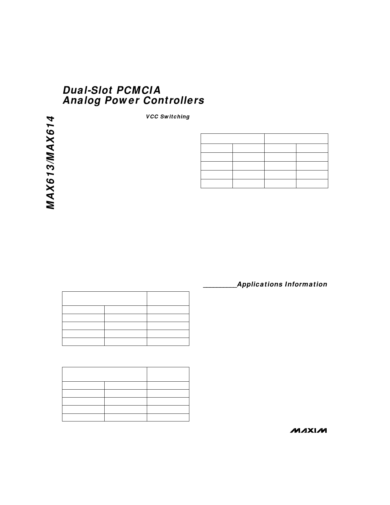
Dual-Slot PCMCIA
Analog Power Controllers
VCC Switching
The MAX613/MAX614 contain level shifters that simplify
driving external power MOSFETs to switch PCMCIA card
VCC. While a PCMCIA card is being inserted into the
socket, the VCC pins on the card edge connector should
be powered down to 0V to prevent “hot insertion” that
may damage the PCMCIA card. The MAX613/MAX614
MOSFET drivers are open drain. Their rise time is con-
trolled by an external pull-up resistor, allowing slow turn-
on of VCC power to the PCMCIA card.
The DRV3 and DRV5 pins on the MAX613 and the DRV
pin on the MAX614 are open-drain outputs pulled down
with internal N-channel devices. The gate drive to
these internal N-channel devices is powered from
VCCIN, regardless of VPPIN’s voltage. If VCCIN is left
unconnected or less than 2V is applied to VCCIN, the
DRV3/DRV5/DRV gate drivers will not sink current.
To switch VCC (M1 and M2 in Figure 1), use external
N-channel power MOSFETs. M1 and M2 should be
logic-level N-channel power MOSFETs with low on
resistance. The Motorola MTP3055EL and Siliconix
Si9956DY MOSFETs are both good choices. Turn on
M1 and M2 by pulling their gates above +5V. With the
gates pulled up to VPPIN as shown in Figure 1, VPPIN
should be at least 10V so that with VCC = 5.5V, M1 and
M2 have at least 4.5V of gate drive.
Table 1. AVPP Control Logic
LOGIC INPUT
AVPP1
0
0
1
1
AVPP0
0
1
0
1
OUTPUT
AVPP
0V
VCCIN
VPPIN
HI-Z
Table 2. BVPP Control Logic
LOGIC INPUT
BVPP1
0
0
1
1
BVPP0
0
1
0
1
OUTPUT
BVPP
0V
VCCIN
VPPIN
HI-Z
Table
Logic
3(–S.—H—MD—ANX=61V3CDCRINV)3
and
DRV5
Control
LOGIC INPUT
VCC1
VCC0
0
0
0
1
1
0
1
1
OUTPUT
DRV3
DRV5
0V
0V
HI-Z
0V
0V
HI-Z
0V
0V
The gates of M1 and M2 can be pulled up to any 10V to
20V source, and do not need to be pulled up to VPPIN.
Typically, the +12V used for VPPIN is supplied from a
+5V to +12V switching regulator. To save power, the
+5V to +12V switching regulator can be shut down
when not using the VPP programming voltage, allowing
VPPIN to fall below +5V.
In this case, M1 and M2 should not be pulled up to
VPPIN, since M1 and M2 cannot be turned on reliably
when VPPIN falls below +10V. Any clock source can
be used to generate a high-side gate-drive voltage by
using capacitors and diodes to build an inexpensive
charge pump. Figure 3 shows a charge-pump circuit
that generates 10V from a +5V logic clock source.
__________Applications Information
The MAX613 contains all the gate drivers and switch-
ing circuitry needed to support a +3.3V/+5V VCC
PCMCIA slot with minimal external components.
Figure 4 shows the analog power control necessary to
support two dual voltage PCMCIA slots. The A:VCC
and B:VCC pins on the Intel 82365SL DF power the
drivers for the control signals that directly connect to
the PCMCIA card.
A 3.3V card needs 3.3V logic-level control signals and
the capability to program VPP1 and VPP2 to 3.3V. The
MAX613’s VCCIN is switched with slot VCC, so AVPP0
= 1 and AVPP1 = 0 causes AVPP = slot VCC.
Likewise, A:VCC and B:VCC are connected to VCCIN,
so the Intel 82365SL DF control signals to the PCMCIA
card are the right logic levels.
PCMCIA card interface controllers other than the
Intel 82365SL DF can be used with Figure 4’s cir-
cuit. Table 4 shows the pins on the Cirrus Logic
CL-PD6720 that perform the same function as the
Intel 82365SL DF pins.
6 _______________________________________________________________________________________
Share Link: 