MC34115 查看數據表(PDF) - Motorola => Freescale
零件编号
产品描述 (功能)
生产厂家
MC34115 Datasheet PDF : 16 Pages
| |||
MC34115
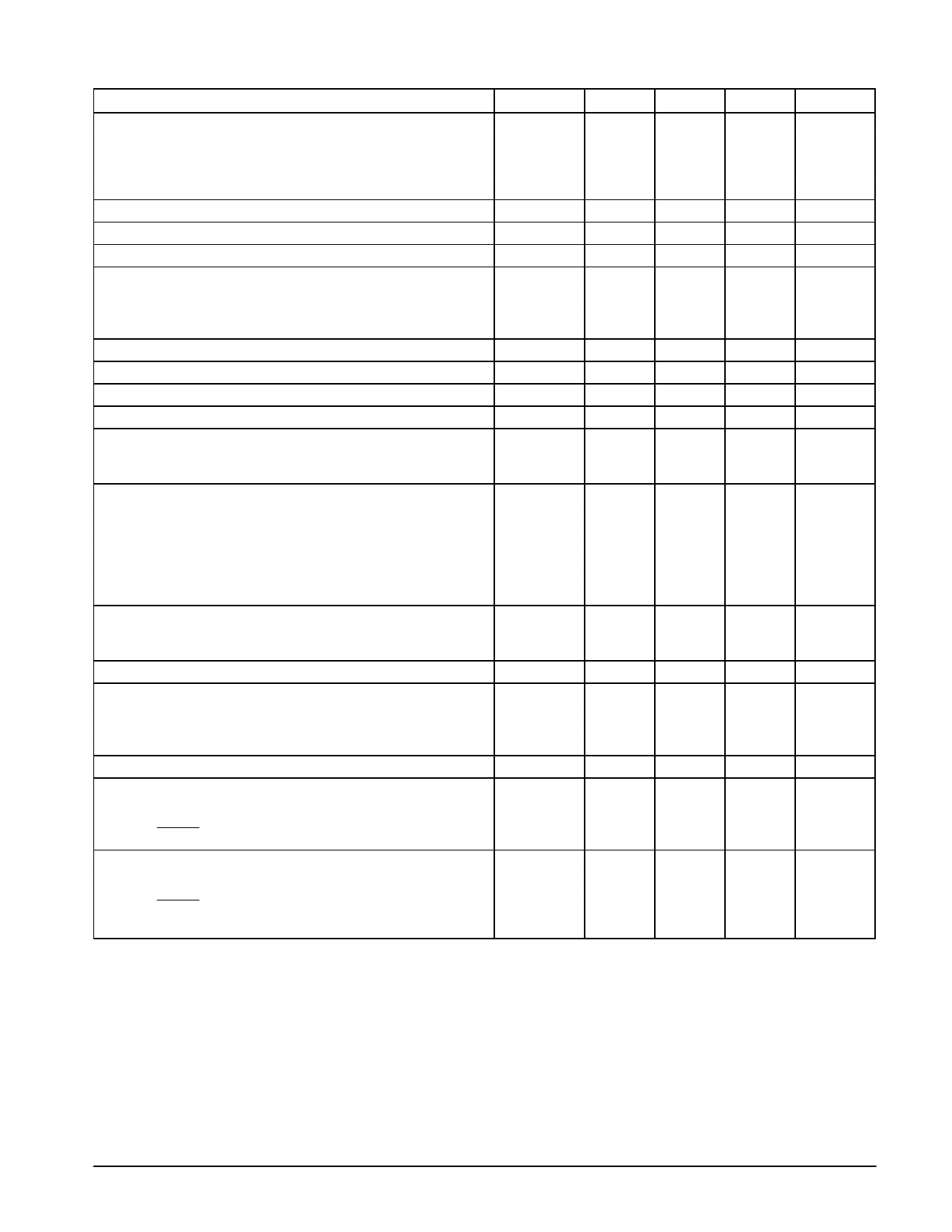
ELECTRICAL CHARACTERISTICS (continued) (VCC = 12 V, VEE = Gnd, TA = 0° to 70°C, unless otherwise noted.)
Characteristic
Symbol
Min
Typ
Max
Propagation Delay Times (Note 1)
Clock Trigger to Digital Output
CL = 25 pF to Gnd
Clock Trigger to Coincidence Output
CL = 25 pF to Gnd, RL = 4.0 kΩ to VCC
Coincidence Output Voltage – Low Logic Stage (IOL(Con) = 3.0 mA)
Coincidence Output Leakage Current – High Logic State (VOH = 15 V)
Applied Digital Threshold Voltage Range (Pin 12)
Digital Threshold Input Current
1.2 V ≤ Vth ≤ VCC – 2.0 V
VIL Applied to Pins 13, 14 and 15
VIH Applied to Pins 13, 14 and 15
Maximum Integrator Amplifier Output Current
VCC/2 Generator Maximum Output Current (Source Only)
VCC/2 Generator Output Impedance (0 to –10 mA)
VCC/2 Generator Tolerance (4.75 V ≤ VCC ≤ 16.5 V)
Logic Input Voltage (Pins 13, 14 and 15)
Low Logic State
High Logic State
Dynamic Total Loop Offset Voltage (Note 3) (Figures 3, 4 and 5)
IGC = 33 µA, VCC = 12 V
TA = 25°C
0°C ≤ TA ≤ +70°C
IGC = 33 µA, VCC = 5.0 V
TA = 25°C
0°C ≤ TA ≤ +70°C
Digital Output Voltage (Pin 9)
IOL = 3.6 mA
IOH = –0.35 mA
Syllabic Filter Applied Voltage (Pin 3) (Figure 2)
Integrating Current (Figure 2)
IGC = 12 µA
IGC = 1.5 mA
IGC = 3.0 mA
Dynamic Integrating Current Match (Figure 6) (IGC = 1.5 mA)
Input Current – High Logic State (VIH = 16.5 V)
Digital Data Input
Clock Input
Encode/Decode Input
tPLH
tPHL
tPLH
tPHL
VOL(Con)
IOH(Con)
Vth
II(th)
IO
Iref
zref
εr
VIL
VIH
ΣVoffset
VOL
VOH
VI(Syl)
IInt
VO(Ave)
IIH
–
1.0
3.0
–
0.8
3.0
–
1.0
3.5
–
0.8
2.5
–
0.12
0.25
–
0.01
0.5
1.2
–
VCC – 2.0
–
–
5.0
–
–10
–50
±5.0
–
–
–10
–
–
–
3.0
6.0
–
–
±3.5
VEE
–
Vth – 0.4
Vth + 0.4
–
16.5
–
±2.5
±7.0
–
±3.0
±10
–
±4.0
±8.0
–
±4.5
±12
–
VCC – 1.0
3.2
0.1
VCC – 0.2
–
0.4
–
VCC
8.0
10
12
1.4
1.5
1.6
2.75
3.0
3.25
–
±100
±300
–
–
5.0
–
–
5.0
–
–
5.0
Input Current – Low Logic State (VIL = 0 V)
Digital Data Input
Clock Input
Encode/Decode Input
Clock Input, VIL = 0.4 V
IIL
–10
–
–
–360
–
–
–36
–
–
–72
–
–
NOTES: 1. All propagation delay times measured 50% to 50% from the negative going (from VCC to +0.4 V) edge of the clock.
2. Devices should not be operated at these values. The “Electrical Characteristics” provide conditions for actual device operation.
3. Dynamic total loop offset (ΣVoffset) equals VIO (comparator) (Figure 3) minus VIOX (Figure 5). The input offset voltages of the analog
comparator and of the integrator amplifier include the effects of input offset current through the input resistors. The slope polarity switch
current mismatch appears as an average voltage across the 10 k integrator resistor. The clock frequency is 16 kHz. Idle channel
performance is guaranteed if this dynamic total loop offset is less than one–half of the change in integrator output voltage during one
clock cycle (ramp step size).
Unit
µs
Vdc
µA
Vdc
µA
mA
mA
Ω
%
Vdc
mV
Vdc
Vdc
µA
mA
mA
mV
µA
µA
MOTOROLA ANALOG IC DEVICE DATA
3
Share Link: 