MC74LCX16373(2010) 查看數據表(PDF) - ON Semiconductor
零件编号
产品描述 (功能)
生产厂家
MC74LCX16373 Datasheet PDF : 7 Pages
| |||
MC74LCX16373
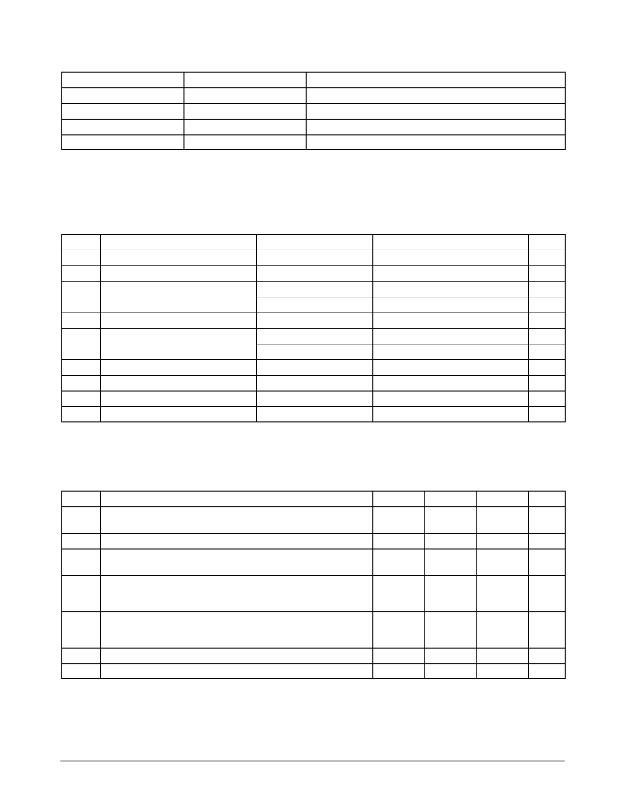
ORDERING INFORMATION
Device
Package
Shipping†
MC74LCX16373DT
TSSOP−48*
39 Units / Rail
MC74LCX16373DTG
TSSOP−48*
39 Units / Rail
MC74LCX16373DTR2
TSSOP−48*
2500 / Tape & Reel
M74LCX16373DTR2G
TSSOP−48*
2500 / Tape & Reel
†For information on tape and reel specifications, including part orientation and tape sizes, please refer to our Tape and Reel Packaging
Specifications Brochure, BRD8011/D.
*This package is inherently Pb−Free.
MAXIMUM RATINGS
Symbol
Parameter
Value
Condition
Unit
VCC DC Supply Voltage
−0.5 to +7.0
V
VI
DC Input Voltage
−0.5 ≤ VI ≤ +7.0
V
VO DC Output Voltage
−0.5 ≤ VO ≤ +7.0
Output in 3−State
V
−0.5 ≤ VO ≤ VCC + 0.5
Output in HIGH or LOW State. (Note 1)
V
IIK
DC Input Diode Current
−50
VI < GND
mA
IOK DC Output Diode Current
−50
VO < GND
mA
+50
VO > VCC
mA
IO
DC Output Source/Sink Current
±50
mA
ICC DC Supply Current Per Supply Pin
±100
mA
IGND DC Ground Current Per Ground Pin
±100
mA
TSTG Storage Temperature Range
−65 to +150
°C
Stresses exceeding Maximum Ratings may damage the device. Maximum Ratings are stress ratings only. Functional operation above the
Recommended Operating Conditions is not implied. Extended exposure to stresses above the Recommended Operating Conditions may affect
device reliability.
1. IO absolute maximum rating must be observed.
RECOMMENDED OPERATING CONDITIONS
Symbol
VCC Supply Voltage
Parameter
Operating
Data Retention Only
Min
Typ
Max
Unit
2.0
2.5, 3.3
3.6
V
1.5
2.5, 3.3
3.6
VI
Input Voltage
VO Output Voltage
0
(HIGH or LOW State)
0
(3−State)
0
5.5
V
VCC
V
5.5
IOH HIGH Level Output Current
VCC = 3.0 V − 3.6 V
VCC = 2.7 V − 3.0 V
VCC = 2.3 V − 2.7 V
IOL LOW Level Output Current
VCC = 3.0 V − 3.6 V
VCC = 2.7 V − 3.0 V
VCC = 2.3 V − 2.7 V
TA
Operating Free−Air Temperature
−55
Dt/DV Input Transition Rise or Fall Rate, VIN from 0.8 V to 2.0 V, VCC = 3.0 V
0
− 24
− 12
−8
+ 24
+ 12
+8
+125
10
mA
mA
°C
ns/V
http://onsemi.com
3
Share Link: 