MJF13007 查看數據表(PDF) - ON Semiconductor
零件编号
产品描述 (功能)
生产厂家
MJF13007 Datasheet PDF : 12 Pages
| |||
MJE13007
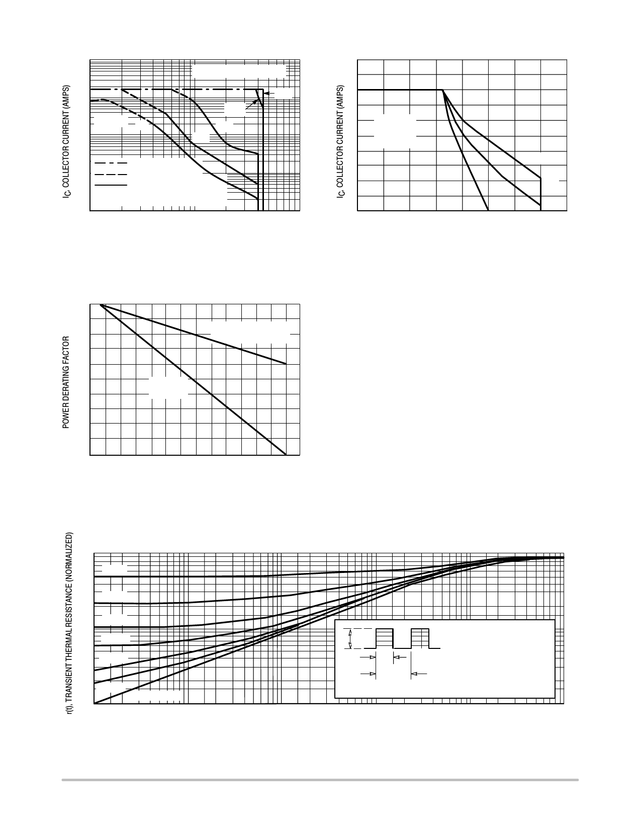
100
50
Extended SOA @ 1 µs, 10 µs
20
10
5
2 TC = 25°C DC
1
0.5
1 µs
10 µs
1 ms
5 ms
0.2
0.1
0.05
0.02
0.01
10
BONDING WIRE LIMIT
THERMAL LIMIT
SECOND BREAKDOWN LIMIT
CURVES APPLY BELOW
RATED VCEO
20 30 50 70 100 200 300 500 1000
VCE, COLLECTOR-EMITTER VOLTAGE (VOLTS)
Figure 6. Maximum Forward Bias
Safe Operating Area
10
8
6
TC ≤ 100°C
GAIN ≥ 4
LC = 500 µH
4
2
VBE(off)
-5 V
0
0V
-2 V
0 100 200 300 400 500 600 700 800
VCEV, COLLECTOR-EMITTER CLAMP VOLTAGE (VOLTS)
Figure 7. Maximum Reverse Bias Switching
Safe Operating Area
1
0.8
SECOND BREAKDOWN
DERATING
0.6
THERMAL
0.4
DERATING
0.2
0
20
40
60 80
100 120 140 160
TC, CASE TEMPERATURE (°C)
Figure 8. Forward Bias Power Derating
There are two limitations on the power handling ability of
a transistor: average junction temperature and second
breakdown. Safe operating area curves indicate IC — VCE
limits of the transistor that must be observed for reliable op-
eration; i.e., the transistor must not be subjected to greater
dissipation than the curves indicate.
The data of Figure 6 is based on TC = 25°C; TJ(pk) is vari-
able depending on power level. Second breakdown pulse
limits are valid for duty cycles to 10% but must be derated
when TC ≥ 25°C. Second breakdown limitations do not der-
ate the same as thermal limitations. Allowable current at the
voltages shown on Figure 6 may be found at any case tem-
perature by using the appropriate curve on Figure 8.
At high case temperatures, thermal limitations will re-
duce the power that can be handled to values less than the
limitations imposed by second breakdown.
Use of reverse biased safe operating area data (Figure 7)
is discussed in the applications information section.
1
0.7 D = 0.5
0.5
D = 0.2
0.2
D = 0.1
0.1
0.07 D = 0.05
0.05
D = 0.02
0.02
D = 0.01
0.01
SINGLE PULSE
0.01 0.02
0.05 0.1
P(pk)
t1
t2
DUTY CYCLE, D = t1/t2
RθJC(t) = r(t) RθJC
RθJC = 1.56°C/W MAX
D CURVES APPLY FOR POWER
PULSE TRAIN SHOWN
READ TIME AT t1
TJ(pk) - TC = P(pk) RθJC(t)
0.2
0.5 1
2
5
10 20
50
t, TIME (msec)
Figure 9. Typical Thermal Response for MJE13007
100 200
500 10Ăk
http://onsemi.com
4
Share Link: 