MJW16206 查看數據表(PDF) - ON Semiconductor
零件编号
产品描述 (功能)
生产厂家
MJW16206 Datasheet PDF : 12 Pages
| |||
MJW16206
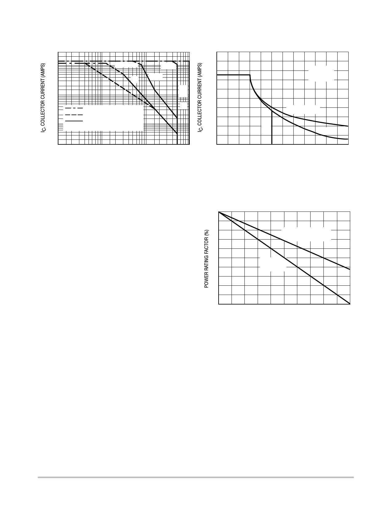
SAFE OPERATING AREA INFORMATION
30
20
20
10
MJW16206
10 µs
16
5
3
dc
5Ăms
2
100
12
1
ns
IC/IB1 ≥ 5
TJ ≤ 100°C
0.5
0.3
WIREBOND LIMIT
0.2
THERMAL LIMIT
0.1
SECONDARY BREAKDOWN
LIMIT
0.05
II*
8
4
VBE(off) = 5 V
0V
2V
0.03
0.02
1
2 3 5 10 20 30 50 100 200 300 500 1K
0
0
200
400
600
800
1K
1.2K
VCE, COLLECTOR-EMITTER VOLTAGE (VOLTS)
VCE, COLLECTOR-EMITTER VOLTAGE (VOLTS)
*REGION II Ċ EXPANDED FBSOA USING
MUR8100E, ULTRAFAST RECTIFIER (SEE FIGURE 12)
Figure 8. Maximum Reverse Bias
Safe Operating Area
Figure 7. Maximum Forward Biased
Safe Operating Area
FORWARD BIAS
There are two limitations on the power handling ability of
a transistor: average junction temperature and second
breakdown. Safe operating area curves indicate IC – VCE
limits of the transistor that must be observed for reliable
operation; i.e., the transistor must not be subjected to greater
dissipation than the curves indicate.
The data of Figure 7 is based on TC = 25_C; TJ(pk) is
variable depending on power level. Second breakdown
pulse limits are valid for duty cycles to 10% but must be
derated when TC ≥ 25_C. Second breakdown limitations do
not derate the same as thermal limitations. Allowable
current at the voltages shown on Figure 7 may be found at
any case temperature by using the appropriate curve on
Figure 9.
At high case temperatures, thermal limitations will reduce
the power that can be handled to values less than the
limitations imposed by second breakdown.
REVERSE BIAS
Inductive loads, in most cases, require the
emitter–to–base junction be reversed biased because high
voltage and high current must be sustained simultaneously
during turn–off. Under these conditions, the collector
voltage must be held to a safe level at or below a specific
value of collector current. This can be accomplished by
several means such as active clamping, RC snubbing, load
100
90
80
70
60
50
40
30
20
10
0
25
SECOND BREAKDOWN
DERATING
THERMAL
DERATING
50
75
100
125
150
TC, CASE TEMPERATURE (°C)
Figure 9. Power Derating
line shaping, etc. The safe level for these devices is specified
as Reverse Biased Safe Operating Area and represents the
voltage–current condition allowable during reverse biased
turn–off. This rating is verified under clamped conditions so
that the device is never subjected to an avalanche mode.
Figure 8 gives the RBSOA characteristics.
http://onsemi.com
4
Share Link: 