ML4801 查看數據表(PDF) - Micro Linear Corporation
零件编号
产品描述 (功能)
生产厂家
ML4801 Datasheet PDF : 14 Pages
| |||
FUNCTIONAL DESCRIPTION (Continued)
VFB
15
2.5V
IAC
2
VRMS
4
ISENSE
3
RAMP 1
8
RTCT
7
16
VEAO
1
IEAO
VEA
-
+
1.6kΩ IEA
+
–
GAIN
MODULATOR
8V
1.6kΩ
POWER FACTOR CORRECTOR
2.75V
PFC
CONTROLLER
-1V
OSCILLATOR
÷2
DUTY CYCLE
LIMIT
OVP
+
-
PFC ILIMIT
+
-
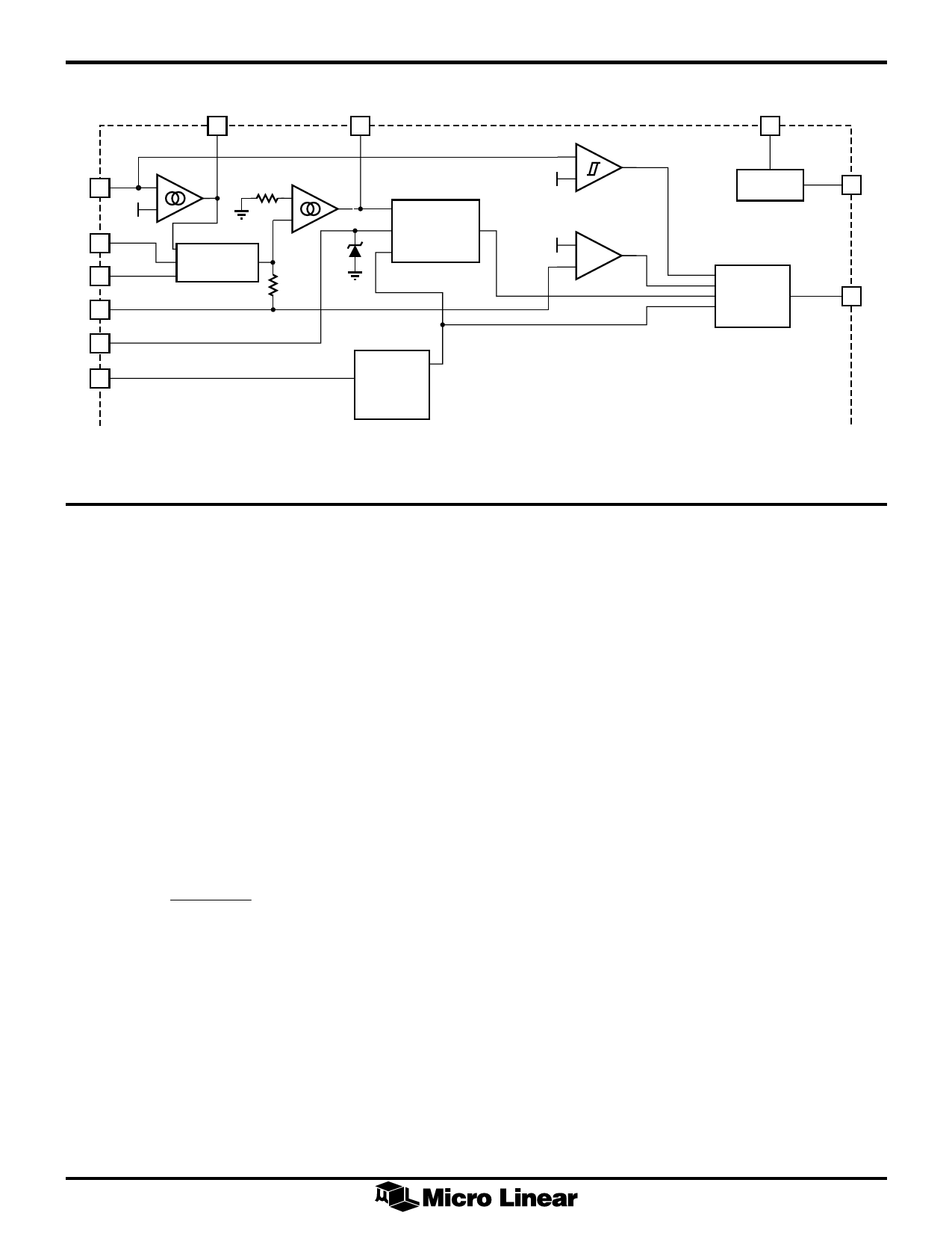
Figure 1. PFC Section Block Diagram
ML4801
13
VCC
7.5V
REFERENCE
VREF
14
PFC
OUTPUT
DRIVER
PFC OUT
12
inversely proportional to VRMS2 (except at unusually
low values of VRMS where special gain contouring
takes over to limit power dissipation of the circuit
components under heavy brownout conditions). The
relationship between VRMS and gain is designated as K.
3) The output of the voltage error amplifier, VEAO. The
gain modulator responds linearly to variations in this
voltage.
The output of the gain modulator is a current signal, in the
form of a full wave rectified sinusoid at twice the line
frequency. This current is applied to the virtual-ground
(negative) input of the current error amplifier. In this way
the gain modulator forms the reference for the current
error loop, and ultimately controls the instantaneous
current draw of the PFC from the power line. The general
form for the output of the gain modulator is:
IGAINMOD
=
IAC ´ VEAO
VRMS 2
´ 1V
More exactly, the output current of the gain modulator is
given by:
IGAINMOD = K × (VEAO − 0.625V) × IAC
(1)
where K is in units of V-1.
Note that the output current of the gain modulator is
limited to ≅ 500µA.
Current Error Amplifier
The current error amplifier’s output controls the PFC duty
cycle to keep the current through the boost inductor a
linear function of the line voltage. At the inverting input
to the current error amplifier, the output current of the
gain modulator is summed with a current which results
from a negative voltage being impressed upon the ISENSE
pin (current into ISENSE ≅ VSENSE/1.6kΩ). The negative
voltage on ISENSE represents the sum of all currents
flowing in the PFC circuit, and is typically derived from a
current sense resistor in series with the negative terminal
of the input bridge rectifier. In higher power applications,
two current transformers are sometimes used, one to
monitor the ID of the boost MOSFET(s) and one to monitor
the IF of the boost diode. As stated above, the inverting
input of the current error amplifier is a virtual ground.
Given this fact, and the arrangement of the duty cycle
modulator polarities internal to the PFC, an increase in
positive current from the gain modulator will cause the
output stage to increase its duty cycle until the voltage on
ISENSE is adequately negative to cancel this increased
current. Similarly, if the gain modulator’s output
decreases, the output duty cycle will decrease to achieve
a less negative voltage on the ISENSE pin.
Cycle-By-Cycle Current Limiter
The ISENSE pin, as well as being a part of the current
feedback loop, is a direct input to the cycle-by-cycle
current limiter for the PFC section. Should the input
voltage at this pin ever be more negative than -1V, the
output of the PFC will be disabled until the protection
flip-flop is reset by the clock pulse at the start of the next
PFC power cycle.
7
Share Link: 