106RH 查看數據表(PDF) - M.S. Kennedy Corporation
零件编号
产品描述 (功能)
生产厂家
106RH Datasheet PDF : 9 Pages
| |||
APPLICATION NOTES
HEAT SINKING
○○○○○○○○○○○
○○○○○○○○○○○○○
CURRENT LIMIT
To select the correct heat sink for your application, refer to the
thermal model and governing equation below.
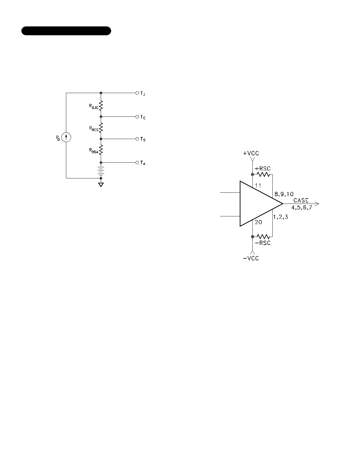
Thermal Model:
The MSK 106RH has an on-board current limit scheme
designed to limit the output drivers anytime output current
exceeds a predetermined limit. The following formula may
be used to determine the value of the current limit resis-
tance necessary to establish the desired current limit.
RSC=
_0_.7_
ISC
Current Limit Connection
Governing Equation:
TJ = PD X (RθJC + RθCS + RθSA) + TA
Where
TJ
PD
RθJC
RθCS
RθSA
TC
TA
TS
= Junction Temperature
= Total Power Dissipation
= Junction to Case Thermal Resistance
= Case to Heat Sink Thermal Resistance
= Heat Sink to Ambient Thermal Resistance
= Case Temperature
= Ambient Temperature
= Sink Temperature
Example:
In our example the amplifier application requires the output to
drive a 10 volt peak sine wave across a 10 ohm load for 1 amp of
output current. For a worst case analysis we will treat the 1 amp
peak output current as a D.C. output current. The power supplies
are ±15 VDC.
1.) Find Power Dissipation
PD=[(quiescent current) X (+VCC - (VCC))] + [(VS - VO) X IOUT]
=(3.5 mA) X (30V) + (5V) X (1A)
=0.1W + 6W
=6.1W
2.) For conservative design, set TJ = +125°C.
3.) For this example, worst case TA = +25°C.
4.) RθJC = 6.0°C/W
5.) Rearrange governing equation to solve for RθSA:
RθSA =(TJ - TA) / PD - (RθJC) - (RθCS)
= (125°C - 25°C) / 6.1W - (6.0°C/W) - (0.15°C/W)
= 10.2°C/W
The heat sink in this example must have a thermal resistance of
no more than 10.2°C/W to maintain a junction temperature of less
than +125°C.
See "Application Circuits" in this data sheet for additional
information on current limit connections.
POWER SUPPLY BYPASSING
Both the negative and the positive power supplies must be
effectively decoupled with a high and low frequency bypass
circuit to avoid power supply induced oscillation. An effec-
tive decoupling scheme consists of a 0.1 microfarad ceramic
capacitor in parallel with a 4.7 microfarad tantalum capacitor
from each power supply pin to ground. It is also a good
practice with high power op-amps, such as the MSK 106RH,
to place a 30-50 microfarad capacitor with a low effective
series resistance, in parallel with the other two power supply
decoupling capacitors. This capacitor will eliminate any peak
output voltage clipping which may occur due to poor power
supply load regulation. All power supply decoupling capaci-
tors should be placed as close to the package power supply
pins as possible.
3
Rev. D 1/05
Share Link: 