NCS2002(2004) 查看數據表(PDF) - ON Semiconductor
零件编号
产品描述 (功能)
生产厂家
NCS2002
(Rev.:2004)
(Rev.:2004)
ON Semiconductor

NCS2002 Datasheet PDF : 16 Pages
| |||
NCS2002, NCV2002
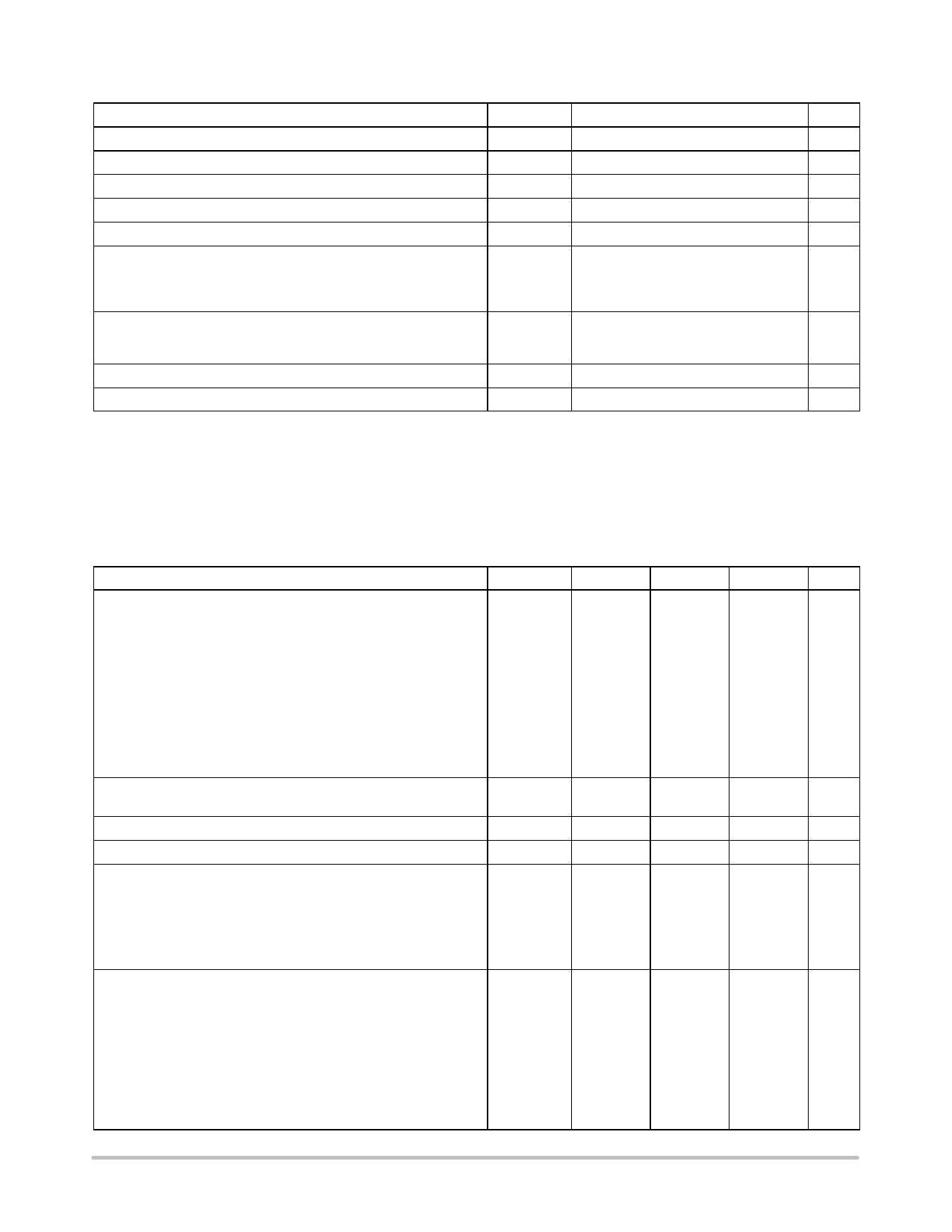
MAXIMUM RATINGS
Rating
Symbol
Value
Unit
Supply Voltage (VCC to VEE)
Input Differential Voltage Range (Note 1)
Input Common Mode Voltage Range (Note 1)
Output Short Circuit Duration (Note 2)
Junction Temperature
Power Dissipation and Thermal Characteristics
SOT23−6 Package
Thermal Resistance, Junction to Air
Power Dissipation @ TA = 70°C
Operating Ambient Temperature Range
NCS2002
NCV2002 (Note 3)
VS
VIDR
VICR
tSc
TJ
RqJA
PD
TA
7.0
VEE – 300 mV to 7.0 V
VEE – 300 mV to 7.0 V
Indefinite
150
235
340
−40 to 105
−40 to 125
V
V
V
sec
°C
°C/W
mW
°C
Storage Temperature Range
Tstg
−65 to 150
°C
ESD Protection at any Pin Human Body Model (Note 4)
VESD
2000
V
1. Either or both inputs should not exceed the range of VEE – 300 mV to VEE + 7.0 V.
2. Maximum package power dissipation limits must be observed to ensure that the maximum junction temperature is not exceeded.
TJTA + (PD RqJA)
3. NCV prefix is for automotive and other applications requiring site and change control.
4. ESD data available upon request.
DC ELECTRICAL CHARACTERISTICS (VCC = 2.5 V, VEE = −2.5 V, VCM = VO = 0 V, RL to Gnd, TA = 25°C, unless otherwise noted)
Rating
Symbol
Min
Typ
Max
Unit
Input Offset Voltage
VCC = 0.45 V, VEE = −0.45 V
TA = 25°C
TA = 0°C to 70°C
TA = Tlow to Thigh
VCC = 1.5 V, VEE = −1.5 V
TA = 25°C
TA = 0°C to 70°C
TA = Tlow to Thigh
VCC = 2.5 V, VEE = −2.5 V
TA = 25°C
TA = 0°C to 70°C
TA = Tlow to Thigh
Input Offset Voltage Temperature Coefficient (RS = 50)
TA = Tlow to Thigh
Input Bias Current (VCC = 1.0 V to 5.0 V)
Input Common Mode Voltage Range
Large Signal Voltage Gain
VCC = 0.45 V, VEE = −0.45 V
RL = 10 k
VCC = 1.5 V, VEE = −1.5 V
RL = 10 k
VCC = 2.5 V, VEE = −2.5 V
RL = 10 k
Output Voltage Swing, High State Output (VID = + 0.5 V)
TA = Tlow to Thigh
VCC = 0.45 V, VEE = −0.45 V
RL = 10 k
RL = 2.0 k
VCC = 1.5 V, VEE = −1.5 V
RL = 10 k
RL = 2.0 k
VCC = 2.5 V, VEE = −2.5 V
RL = 10 k
RL = 2.0 k
VIO
−6.0
0.5
6.0
−8.5
−
8.5
−9.5
−
9.5
−6.0
0.5
6.0
−7.0
−
7.0
−7.5
−
7.5
−6.0
0.5
6.0
−7.5
−
7.5
−7.5
−
7.5
DVIO / DT
−
8.0
−
IIB
VICR
AVOL
VOH
−
10
−
−
VEE to VCC
−
−
40
−
−
40
−
10
40
−
0.40
0.442
−
0.35
0.409
−
1.45
1.494
−
1.40
1.473
−
2.45
2.493
−
2.40
2.469
−
mV
mV/°C
pA
V
kV/V
V
http://onsemi.com
2
Share Link: