NJM4151(2003) 查看數據表(PDF) - Japan Radio Corporation
零件编号
产品描述 (功能)
生产厂家
NJM4151 Datasheet PDF : 10 Pages
| |||
NJM4151
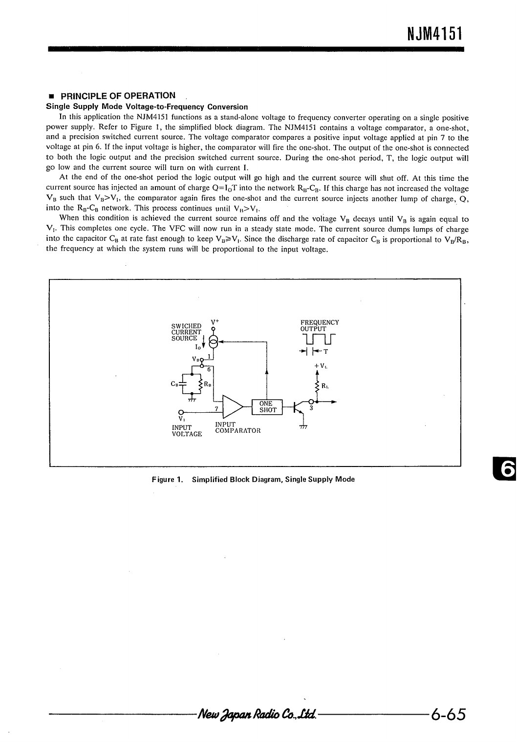
■ PRINCIPLE OF OPERATION
Single Supply Mode Voltage-to-Frequency Conversion
In this application the NJM4151 functions as a stand-alone voltage to frequency converter operating on a single positive
power supply. Refer to Figure 1, the simplified block diagram. The NJM4151 contains a voltage comparator, a one-shot,
and a precision switched current source. The voltage comparator compares a positive input voltage applied at pin 7 to the
voltage at pin 6. If the input voltage is higher, the comparator will fire the one-shot. The output of the one-shot is
connected to both the logic output and the precision switched current source. During the one-shot period, T, the logic
output will go low and the current source will turn on with current I.
At the end of the one-shot period the logic output will go high and the current source will shut off. At this time the current
source has injected an amount of charge Q = I0T into the network RB-CB. If this charge has not increased the voltage VB
such that VB > VI, the comparator again fires the one-shot and the current source injects another lump of charge, Q, into
the RB-CB network. This process continues until VB > VI.
When this condition is achieved the current source remains off and the voltage VB decays until VB is again equal to VI.
This completes one cycle. The VFC will now run in a steady state mode. The current source dumps lumps of charge into
the capacitor CB at rate fast enough to keep VB ≥ VI. Since the discharge rate of capacitor CB is proportional to VB/RB, the
frequency at which the system runs will be proportional to the input voltage.
Figure 1. Simplified Block Diagram, Single Supply Mode
The NJM4151 VFC is easy to use and apply if you understand the operation of it through the block diagram, Figure
1. Many users, though, have expressed the desire to understand the workings of the internal circuitry. The circuit can be
divided into five sections: the internal biasing network, input comparator, one-shot, voltage reference, and the output
current source.
The internal biasing network is composed of Q39-Q43. The N-channel FET Q43 supplies the initial current for zener
diode Q39. The NPN transistor Q38 senses the zener voltage to derive the current reference for the multiple collector
current source Q41. This special PNP transistor provides active pull-up for all of the other sections of the NJM4151.
The input comparator section is composed of Q1-Q7. Lateral PNP transistors Q1-Q4 form the special
ground-sensing input which is necessary for VFC operation at low input voltages, NPN transistors Q5 and Q6 convert the
differential signal to drive the second gain stage Q7. If the voltage on input pin 7 is less than that on threshold pin 6, the
comparator will be off and the collector of Q7 will be in the high state. As soon as the voltage on pin 7 exceeds the voltage
on pin 6, the collector of Q7 will go low and trigger the one-shot.
Ver.2003-12-09
-3-
Share Link: 