NT3967 查看數據表(PDF) - Unspecified
零件编号
产品描述 (功能)
生产厂家
NT3967 Datasheet PDF : 11 Pages
| |||
NT3967
TFT LCD Source Driver
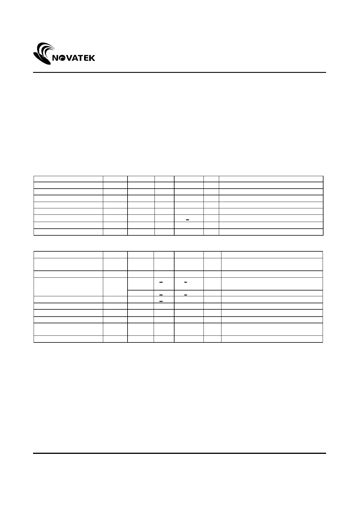
Absolute Maximum Ratings*
*Comments
Digital supply voltage, Vcc
-0.5V to 5V
Analog supply voltage, AVDD
-0.5V to +11V
Supply voltage, V1~ V10
-0.3 ~AVDD+0.3
Digital input voltage
-0.5V to Vcc+0.5V
Output voltage, DIO1 & DIO2 -0.5V to Vcc+0.5V
Output voltage,OUT1~OUT420 -0.5V to AVDD+0.5V
Storage temperature
-55℃ to 100℃
Operating temperature
-10℃ to 75℃
Stresses above those listed under "Absolu te Maximum
Ratings" may cause permanent damage to the device.
These are stress ratings only. Functional operation of this
device at these or under any other conditions above those
indicated in the operational sections of this specification are
not implied and exposure to absolute maximum rating
conditions for extended periods may affect device reliability.
DC Electrical Characteristics (Vcc =2.5~3.6V , AVDD=6.5~10V, AVSS=GND=0V, TA=-10℃~75℃)
(For the digital circuit)
Parameter
Symbol Min. Typ. Max. Unit
Conditions
Supply Voltage
Vcc
2.5
-
3.6
V Digital power
Low Level Input Voltage
Vil
0
-
0.3xVcc V For the digital circuit
High Level Input Voltage
Vih 0.7xVcc -
Vcc
V For the digital circuit
High Level Output Voltage Voh Vcc-0.3V -
-
V DIO1/2, Ioh=500uA
Low Level Output Voltage
Vol
-
- GND+0.3V V DIO1/2, Iol=-500uA
Input Leakage Current
Ii
-
-
+1
µA For the digital circuit
Digital Stand-by current
Ist
-
-
50
µA CLK is stopped, DIO1/2 No load
Digital Operating Current
Icc
-
3
5
mA Fclk=40 MHz, FLD=50KHz
(For the analog circuit)
Parameter
Symbol Min. Typ. Max. Unit
Supply Voltage
AVDD
6.5
8.4
10
V
Input level of V1 ~ V5
Vref 0.4AVDD - AVDD-0.1 V
Input level of V6 ~ V10
Vref
0.1
0.6AVDD V
Voltage Output Deviation
Vvd
-
+20
+25
mV
+10
+20
mV
Voltage Output Offset
Voc
+10
mV
Dynamic Range of Output Vdr
0.1
- AVDD-0.1 V
Sinking Current of outputs IOL
-150 -180
-
µA
Driving Current of outputs
IOH
150 200
-
µA
Impedance of Gamma
Ri
0.8*Rn Rn 1.3*Rn
ohm
Correction
Analog Operating Current IDD
-
3
6
mA
Conditions
For the analog circuit power
Gamma correction voltage
Gamma correction voltage
Vo=0.1V ~ 1.5V & AVDD-1.5 ~ AVDD-
0.1V
Vo=1.5V ~ AVDD-1.5V
OUT1 ~ OUT402
OUT1 ~ OUT402; Vo=0.1V V.S 1.1V
OUT1 ~ OUT402; Vo=9.9V V.S 8.9V
Rn=15850 ohm, from V1 ~ V5 & V6~V10
No load, Fclk=33MHz, FLD=50KHz
Version 1.0
8
DEC 7,2001
Share Link: 