NT5SV16M4DT 查看數據表(PDF) - Unspecified
零件编号
产品描述 (功能)
生产厂家
NT5SV16M4DT Datasheet PDF : 21 Pages
| |||
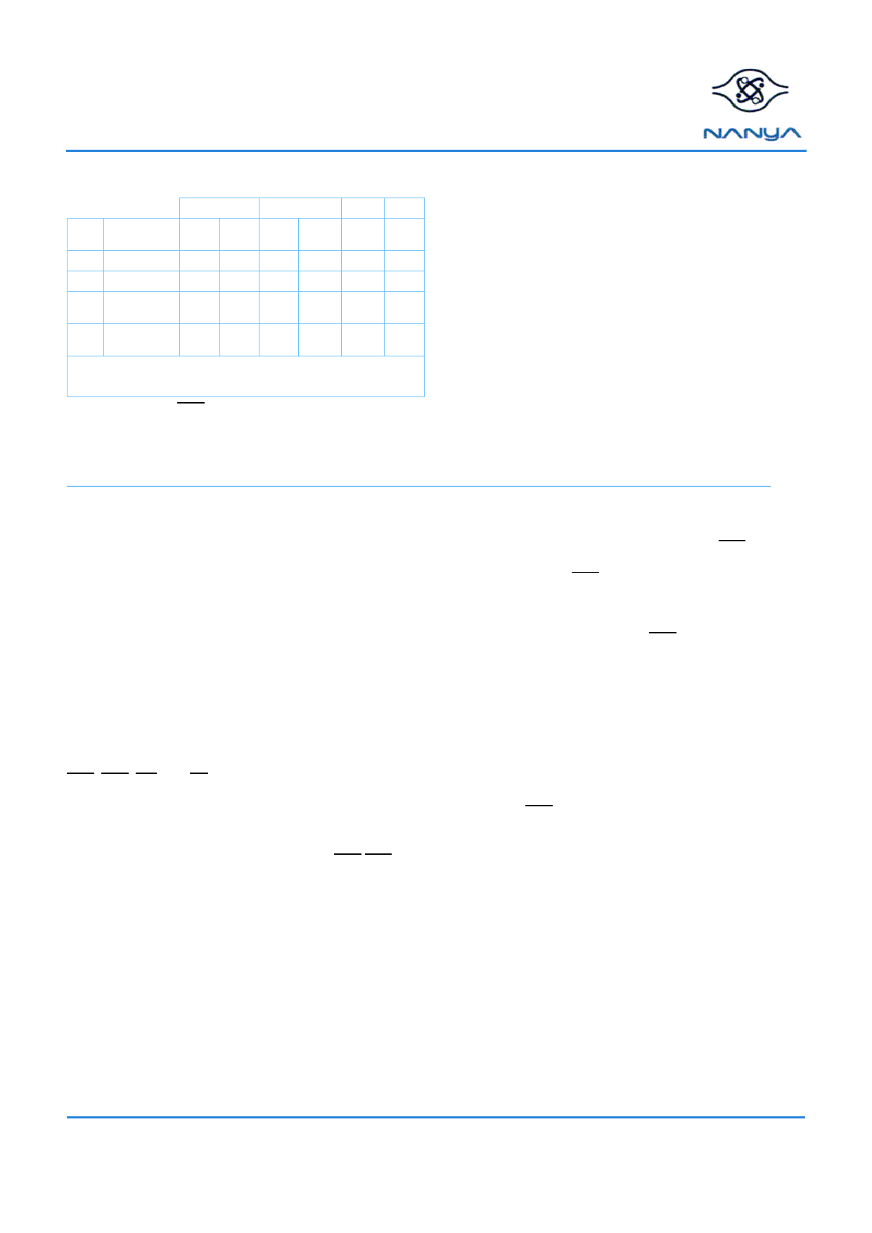
NT5SV16M4DT
NT5SV8M8DT
NT5SV4M16DT
64Mb Synchronous DRAM
Features
• High Performance:
-6K
-7K
fCK
Clock
Frequency
166 133 143 133
tCK Clock Cycle
6
7.5
7
7.5
CL CAS Latency CL=3 CL=2 CL=3 CL=2
tAC
Clock Access
Time1
---
—
--- —
tAC
Clock Access
Time2
5.4
5.4
5.4
5.4
-7
143
7
CL=3
—
5.4
Units
MHz
ns
CKs
ns
ns
1. Terminated load. See AC Characteristics on page 16.
2. Unterminated load. See AC Characteristics on page 16.
• Single Pulsed RAS Interface
• Fully Synchronous to Positive Clock Edge
• Four Banks controlled by BS0/BS1 (Bank Select)
• Programmable CAS Latency: 2, 3
• Programmable Burst Length: 1, 2, 4, 8, Full page
• Programmable Wrap: Sequential or Interleave
• Multiple Burst Read with Single Write Option
• Automatic and Controlled Precharge Command
• Data Mask for Read/Write control (x4, x8)
• Dual Data Mask for byte control (x16)
• Auto Refresh (CBR) and Self Refresh
• Suspend Mode and Power Down Mode
• Standard Power operation
• 4096 refresh cycles/64ms
• Random Column Address every CK (1-N Rule)
• Single 3.3V ± 0.3V Power Supply
• LVTTL compatible
• Package: 54-pin 400 mil TSOP-Type II
Description
The NT5SV16M4DT, NT5SV8M8DT, and NT5SV4M16DT
are four-bank Synchronous DRAMs organized as 4Mbit x 4
I/O x 4 Bank, 2Mbit x 8 I/O x 4 Bank, and 1Mbit x 16 I/O x 4
Bank, respectively. These synchronous devices achieve
high-speed data transfer rates of up to 200MHz by employing
a pipeline chip architecture that synchronizes the output data
to a system clock. The chip is fabricated with NTC’s
advanced 64Mbit single transistor CMOS DRAM process
technology.
The device is designed to comply with all JEDEC standards
set for synchronous DRAM products, both electrically and
mechanically. All of the control, address, and data input/out-
put (I/O or DQ) circuits are synchronized with the positive
edge of an externally supplied clock.
RAS, CAS, WE, and CS are pulsed signals which are exam-
ined at the positive edge of each externally applied clock
(CK). Internal chip operating modes are defined by combina-
tions of these signals and a command decoder initiates the
necessary timings for each operation. A fourteen bit address
bus accepts address data in the conventional RAS/CAS mul-
tiplexing style. Twelve row addresses (A0-A11) and two bank
select addresses (BS0, BS1) are strobed with RAS. Eleven
column addresses (A0-A9) plus bank select addresses and
A10 are strobed with CAS. Column address A9 is dropped on
the x8 device, and column addresses A8 and A9 are dropped
on the x16 device.
Prior to any access operation, the CAS latency, burst length,
and burst sequence must be programmed into the device by
address inputs A0-A11, BS0, BS1 during a mode register set
cycle. In addition, it is possible to program a multiple burst
sequence with single write cycle for write through cache oper-
ation.
Operating the four memory banks in an interleave fashion
allows random access operation to occur at a higher rate
than is possible with standard DRAMs. A sequential and gap-
less data rate of up to 200MHz is possible depending on
burst length, CAS latency, and speed grade of the device.
Simultaneous operation of both decks of a stacked device is
allowed, depending on the operation being done. Auto
Refresh (CBR) and Self Refresh operation are supported.
REV 1.1
10/01
1
© NANYA TECHNOLOGY CORP. All rights reserved.
NANYA TECHNOLOGY CORP. reserves the right to change Products and Specifications without notice.
Share Link: 