RMM2080 查看數據表(PDF) - Fairchild Semiconductor
零件编号
产品描述 (功能)
生产厂家
RMM2080 Datasheet PDF : 5 Pages
| |||
Electrical Characteristics (at 25°C)
50Ω system, Vd = +7V, quiescent current (Idq) = 300 mA, GC1, GC2 = +1.5V
Parameter
Frequency Range
Gate Supply Voltage (Vg)1
RF Output Power @ -1dB
Small Signal Gain
Gain Flatness vs. Freq.
Input/Output Return Loss
Gain Control Range
Gain Control Voltage, GC1&22
Min
Typ
2
–
-0.7
20
18
24
±2
7
70
-5
Notes:
1. Typical range of the negative gate voltage is -0.9 to 0.0V to set typical Idq of 300 mA.
2. GC1 and GC2 of +1.5V and VG23 = open corresponds to maximum gain and power.
Max
18
+1.5
Units
GHz
V
dBm
dB
dB
dB
dB
V
VG1 GC1 GC2
VDD
VG23
RF IN
RF OUT
0.127
0.122
0.118
0.114
0.100
VG1 GC1
GC2
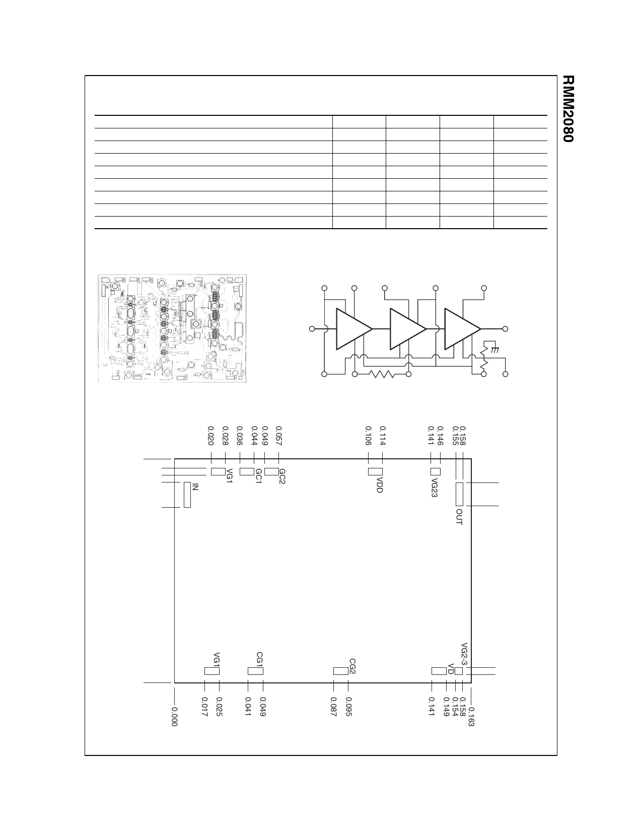
Figure 1. Block Diagram and Circuit Schematic
VD VG2-3
0.114
0.100
RMM2080
0.000
0.009
0.005
Figure 2. Location and Size of Bonding Pads (Dimensions in Inches)
©2004 Fairchild Semiconductor Corporation
RMM2080 Rev. C
Share Link: 