SMAJ70(V2) 查看數據表(PDF) - Galaxy Semi-Conductor
零件编号
产品描述 (功能)
生产厂家
SMAJ70 Datasheet PDF : 4 Pages
| |||
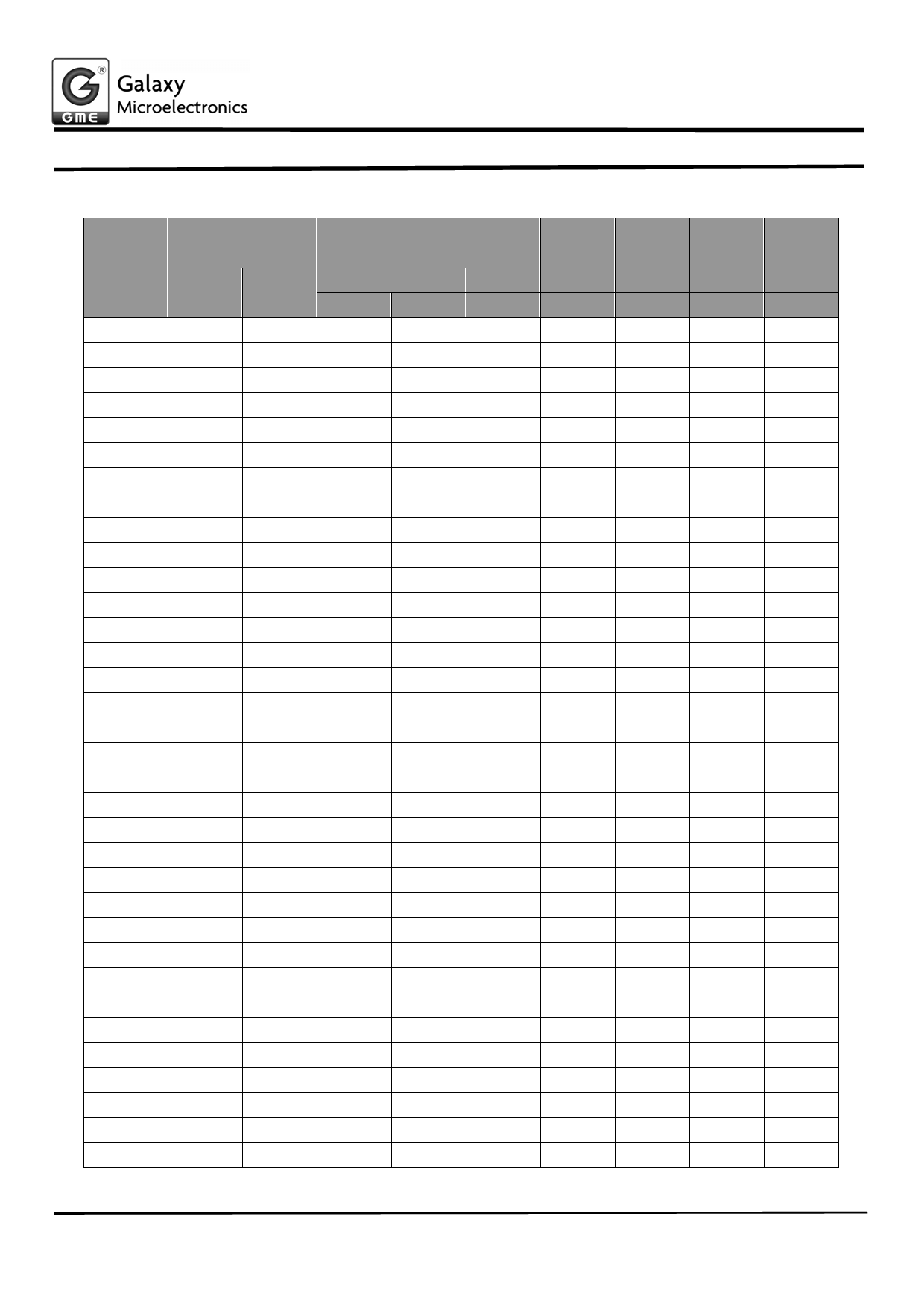
ELECTRICAL CHARACTERISTICS
R atings at 25 am bient tem perature unles s otherwis e spec if ied.VF=3.5V at IF=25A (uni-directional only )
Device ty pe
De v ic e
marking
code
Uni
Bi
Breakdow n
v oltage V (BR) at IT(1)
(V)
Min
Max
Te s t
current
IT(m A )
Stand-of f
v oltage
VWM (V)
Max imum
reverse leakage
at V WM
ID( A )(3)
Max imum
peak pulss surge
current I PPM
(A )(2)
Max imum
clamping
v oltage at I PPM
Vc (V)
SMA J5.0
AD
WD
6.40
7.81
10
5.0
800
SMA J5.0A (5) A E
WE
6.40
7.08
10
5.0
800
SMA J6.0
AF
WF
6.67
8.15
10
6.0
800
SMA J6.0A
AG
WG
6.67
7.37
10
6.0
800
SMA J6.5
AH
WH
7.22
8.82
10
6.5
500
SMA J6.5A
AK
WK
7.22
7.98
10
6.5
500
SMA J7.0
AL
WL
7.78
9.51
10
7.0
200
SMA J7.0A
AM
WM
7.78
8.60
10
7.0
200
SMA J7.5
AN
WN
8.33
10.3
1.0
7.5
100
SMA J7.5A
AP
WP
8.33
9.21
1.0
7.5
100
SMA J8.0
AQ
WQ
8.89
10.9
1.0
8.0
50
SMA J8.0A
AR
WR
8.89
9.83
1.0
8.0
50
SMA J8.5
AS
WS
9.44
11.5
1.0
8.5
10
SMA J8.5A
AT
WT
9.44
10.4
1.0
8.5
10
SMA J9.0
AU
WU
10.0
12.2
1.0
9.0
5.0
SMA J9.0A
AV
WV
10.0
11.1
1.0
9.0
5.0
SMA J10
AW
WW
11.1
13.6
1.0
10
5.0
SMA J10A
AX
WX
11.1
12.3
1.0
10
5.0
SMA J11
AY
WY
12.2
14.9
1.0
11
5.0
SMA J11A
AZ
WZ
12.2
13.5
1.0
11
5.0
SMA J12
BD
XD
13.3
16.3
1.0
12
5.0
SMA J12A
BE
XE
13.3
14.7
1.0
12
5.0
SMA J13
BF
XF
14.4
17.6
1.0
13
5.0
SMA J13A
BG
XG
14.4
15.9
1.0
13
5.0
SMA J14
BH
XH
15.6
19.1
1.0
14
5.0
SMA J14A
BK
XK
15.6
17.2
1.0
14
5.0
SMA J15
BL
XL
16.7
20.4
1.0
15
5.0
SMA J15A
BM
XM
16.7
18.5
1.0
15
5.0
SMA J16
BN
XN
17.8
21.8
1.0
16
5.0
SMA J16A
BP
XP
17.8
19.7
1.0
16
5.0
SMA J17
BQ
XQ
18.9
23.1
1.0
17
5.0
SMA J17A
BR
XR
18.9
20.9
1.0
17
5.0
SMA J18
BS
XS
20.0
24.4
1.0
18
5.0
SMA J18A
BT
XT
20.0
22.1
1.0
18
5.0
SMA J20
BU
XU
22.2
27.1
1.0
20
5.0
SMA J20A
BV
XV
22.2
24.5
1.0
20
5.0
SMA J22
BW
XW
24.4
29.8
1.0
22
5.0
SMA J22A
BX
XX
24.4
26.9
1.0
22
5.0
SMA J24
BY
XY
26.7
32.6
1.0
24
5.0
SMA J24A
BZ
XZ
26.7
29.5
1.0
24
5.0
SMA J26
CD
YD
28.9
35.3
1.0
26
5.0
SMA J26A
CE
YE
28.9
31.9
1.0
26
5.0
SMA J28
CF
YF
31.1
38.0
1.0
28
5.0
SMA J28A
CG
YG
31.1
34.4
1.0
28
5.0
SMA J30
CH
YH
33.3
40.7
1.0
30
5.0
SMA J30A
CK
YK
33.3
36.8
1.0
30
5.0
Notes : (1) Pulse test :tP 50ms
(2) Surge c urrent w avef orm per Fig.3 and derate per Fig.2
(3) For bi-direc tional types hav ing V WM of 10 V olts and less ,the ID Iimit is doubled
(4) A ll terms and sy mbols are c onsistent w ith A NSI/IEEE C62.35
(5) For the bidirectional SMA J5.0CA ,the maximum V (BR) is 7.25V
41.7
43.5
35.1
38.8
32.5
35.7
30.1
33.3
28.0
31.0
26.7
29.4
25.2
27.8
23.7
26.0
21.3
23.5
19.9
22.0
18.2
20.1
16.8
18.6
15.5
17.2
14.9
16.4
13.9
15.4
13.1
14.5
12.4
13.7
11.2
12.3
10.2
11.3
9.3
10.3
8.6
9.5
8.0
8.8
7.5
8.3
9.6
9.2
11.4
10.3
12.3
11.2
13.3
12.0
14.3
12.9
15.0
13.6
15.9
14.4
16.9
15.4
18.8
17.0
20.1
18.2
22.0
19.9
23.8
21.5
25.8
23.2
26.9
24.4
28.8
26.0
30.5
27.6
32.2
29.2
35.8
32.4
39.4
35.5
43.0
38.9
46.6
42.1
50.0
45.4
53.5
48.4
www.galaxycn.com
Document Number 0285005
BLGALAXY ELECTRICAL
2.
Share Link: 