ADP3402 查看數據表(PDF) - Analog Devices
零件编号
产品描述 (功能)
生产厂家
ADP3402 Datasheet PDF : 12 Pages
| |||
a
GSM Power Management System
ADP3402
FEATURES
Handles all GSM Baseband Power Management
Functions
Four LDOs Optimized for Specific GSM Subsystems
Charges Back-Up Capacitor for Real-Time Clock
Charge Pump and Logic Level Translators for 3 V and 5 V
GSM SIM Modules
Thermally Enhanced 6.1 mm 28-Lead TSSOP Package
APPLICATIONS
GSM/DCS/PCS Handsets
TeleMatic Systems
ICO/Iridium Terminals
GENERAL DESCRIPTION
The ADP3402 is a multifunction power management system IC
optimized for GSM cell phones. The wide input voltage range of
3.0 V to 7.0 V makes the ADP3402 ideal for both single cell
Li-Ion and three cell NiMH designs. The current consumption of
the ADP3402 has been optimized for maximum battery life,
featuring a ground current of only 230 µA when the phone is in
standby (digital LDO, analog LDO, and SIM card supply active).
An undervoltage lockout (UVLO) prevents the startup when
there is not enough energy in the battery. All four integrated
LDOs are optimized to power one of the critical sub-blocks of the
phone. Their novel anyCAP™ architecture requires only very
small output capacitors for stability, and the LDOs are insensitive
to the capacitors’ equivalent series resistance (ESR). This makes
them stable with any capacitor, including ceramic (MLCC) types
for space-restricted applications.
A step-up converter is implemented to supply both the SIM
module and the level translation circuitry to adapt logic signals
for 3 V and 5 V SIM modules. Sophisticated controls are avail-
able for power-up during battery charging, keypad interface and
charging of an auxiliary back-up capacitor for the real-time clock.
These allow an easy interface between ADP3402, GSM proces-
sor, charger, and keypad. The 28-lead TSSOP package has been
thermally enhanced to maximize power dissipation capability.
Furthermore, a reset circuit and a thermal shutdown function
have been implemented to support reliable system design.
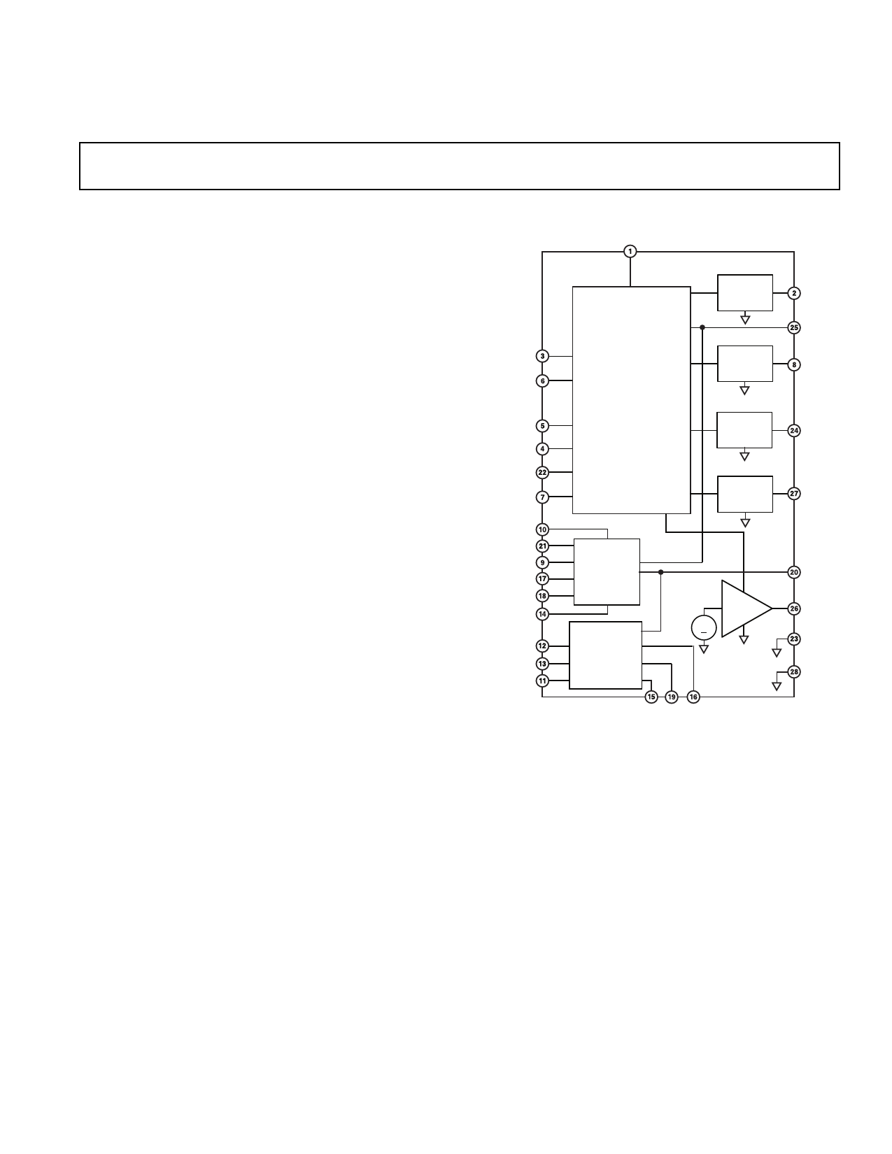
FUNCTIONAL BLOCK DIAGRAM
VBAT
ADP3402
DIGITAL
LDO
PWRONKEY
ROWX
PWRONIN
ANALOGON
RESCAP
CHRON
SIMBAT
CAP+
CAP؊
SIMPROG
SIMON
SIMGND
RESETIN
CLKIN
DATAIO
POWER-UP
SEQUENCING
AND
PROTECTION
LOGIC
RTC LDO
XTAL OSC
LDO
ANALOG
LDO
CHARGE
PUMP
LOGIC LEVEL
TRANSLATION
REF
+
BUFFER
I/O CLK RST
VCC
RESET
VRTC
VTCXO
VCCA
VSIM
REFOUT
DGND
AGND
anyCAP is a trademark of Analog Devices, Inc.
REV. 0
Information furnished by Analog Devices is believed to be accurate and
reliable. However, no responsibility is assumed by Analog Devices for its
use, nor for any infringements of patents or other rights of third parties
which may result from its use. No license is granted by implication or
otherwise under any patent or patent rights of Analog Devices.
One Technology Way, P.O. Box 9106, Norwood, MA 02062-9106, U.S.A.
Tel: 781/329-4700 World Wide Web Site: http://www.analog.com
Fax: 781/326-8703
© Analog Devices, Inc., 2000
Share Link: 