VN920SOTR-E 查看數據表(PDF) - STMicroelectronics
零件编号
产品描述 (功能)
生产厂家
VN920SOTR-E Datasheet PDF : 24 Pages
| |||
VN920-E / VN920B5-E / VN920SO-E
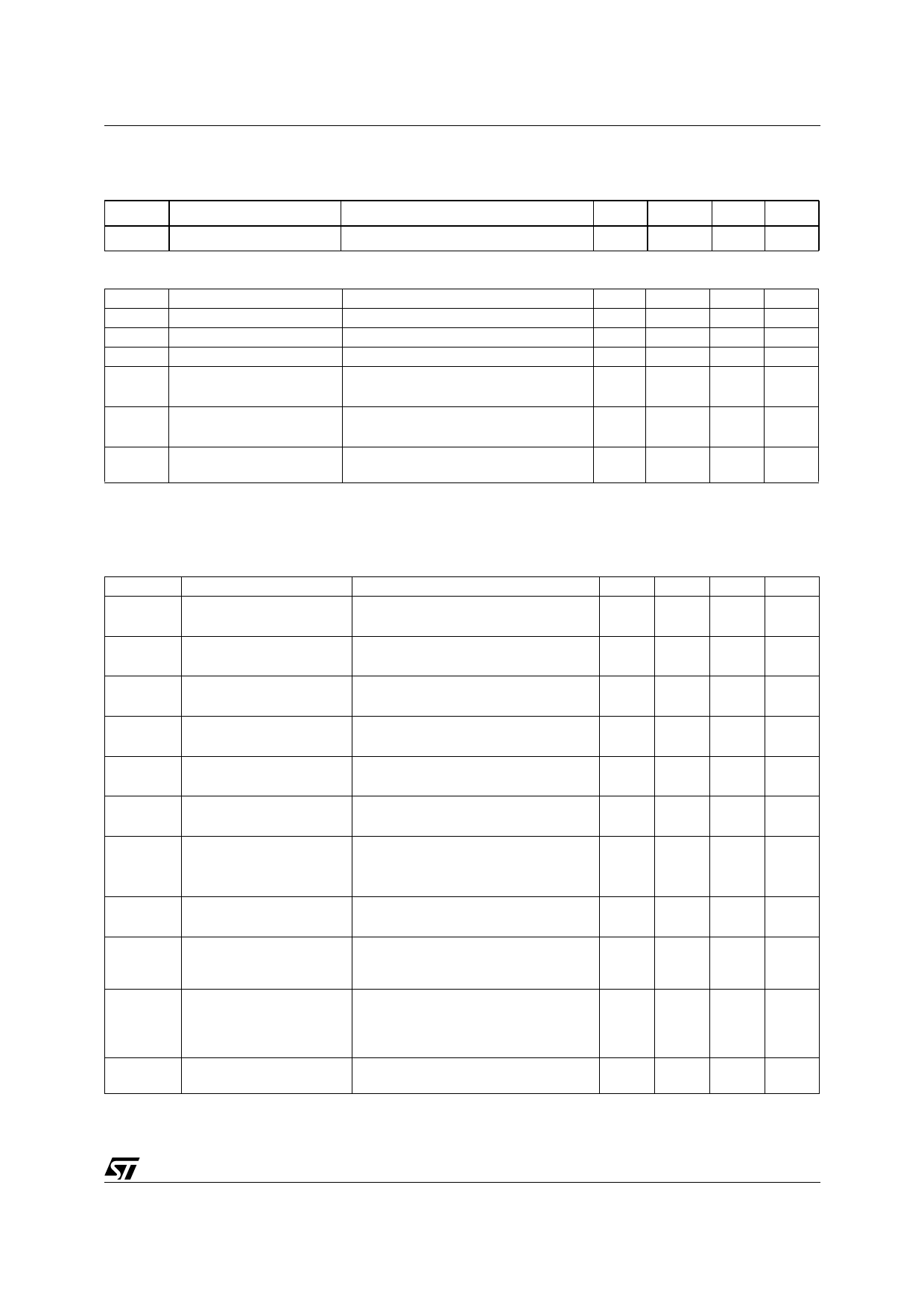
ELECTRICAL CHARACTERISTICS (continued)
Table 8. VCC - Output Diode
Symbol
Parameter
VF
Forward on Voltage
Test Conditions
-IOUT=2A; Tj=150°C
Min.
Typ.
Max. Unit
0.6
V
Table 9. Protections (see note 1)
Symbol
TTSD
TR
Thyst
Parameter
Shut-down Temperature
Reset Temperature
Thermal Hysteresis
Ilim DC Short Circuit Current
Vdemag
VON
Turn-off Output Clamp
Voltage
Output Voltage Drop
Limitation
Test Conditions
VCC=13V
5V<VCC<36V
IOUT=2A; VIN=0V; L=6mH
IOUT=1A; Tj=-40°C....+150°C
Min
Typ
Max Unit
150
175
200
°C
135
°C
7
15
°C
30
45
75
A
75
A
VCC-41 VCC-48 VCC-55 V
50
mV
Note: 1. To ensure long term reliability under heavy overload or short circuit conditions, protection and related diagnostic signals must be
used together with a proper software strategy. If the device is subjected to abnormal conditions, this software must limit the duration
and number of activation cycles.
Table 10. Current Sense (9V≤VCC≤16V) (See Fig. 5)
Symbol
K1
dK1/K1
K2
dK2/K2
K3
dK3/K3
Parameter
IOUT/ISENSE
Current Sense Ratio Drift
IOUT/ISENSE
Current Sense Ratio Drift
IOUT/ISENSE
Current Sense Ratio Drift
Test Conditions
IOUT=1A; VSENSE=0.5V;
Tj= -40°C...150°C
IOUT=1A; VSENSE=0.5V;
Tj= -40°C...+150°C
IOUT=10A; VSENSE=4V; Tj=-40°C
Tj=25°C...150°C
IOUT=10A; VSENSE=4V;
Tj=-40°C...+150°C
IOUT=30A; VSENSE=4V; Tj=-40°C
Tj=25°C...150°C
IOUT=30A; VSENSE=4V;
Tj=-40°C...+150°C
Min Typ Max Unit
3300 4400 6000
-10
+10
%
4200
4400
4900
4900
6000
5750
-8
+8
%
4200
4400
4900
4900
5500
5250
-6
+6
%
ISENSEO
Analog Sense Leakage
Current
VCC=6...16V; IOUT=0A;VSENSE=0V;
Tj=-40°C...+150°C
0
10
µA
VSENSE
VSENSEH
RVSENSEH
tDSENSE
Max Analog Sense Output
Voltage
Sense Voltage in
Overtemperature
conditions
Analog Sense Output
Impedance in
Overtemperature
Condition
Current sense delay
response
VCC=5.5V; IOUT=5A; RSENSE=10KΩ
VCC>8V; IOUT=10A; RSENSE=10KΩ
VCC=13V; RSENSE=3.9KΩ
VCC=13V; Tj>TTSD; Output Open
to 90% ISENSE (see note 2)
2
V
4
V
5.5
V
400
Ω
500
µs
Note: 2. current sense signal delay after positive input slope.
5/24
Share Link: 