LT1223CN8 查看數據表(PDF) - Linear Technology
零件编号
产品描述 (功能)
生产厂家
LT1223CN8 Datasheet PDF : 16 Pages
| |||
LT1223
ABSOLUTE AXI U RATI GS
(Note 1)
Supply Voltage ...................................................... ±18V
Differential Input Voltage ......................................... ±5V
Input Voltage ............................ Equal to Supply Voltage
Output Short Circuit Duration (Note 2) ......... Continuous
Operating Temperature Range
LT1223M (OBSOLETE) .............. –55°C to 125°C
LT1223C ................................................ 0°C to 70°C
Storage Temperature Range ..................–65°C to 150°C
Junction Temperature Plastic Package ........... 150°C
Junction Temperature Ceramic Package
(OBSOLETE) ..................................... 175°C
Lead Temperature (Soldering, 10 sec.)................. 300°C
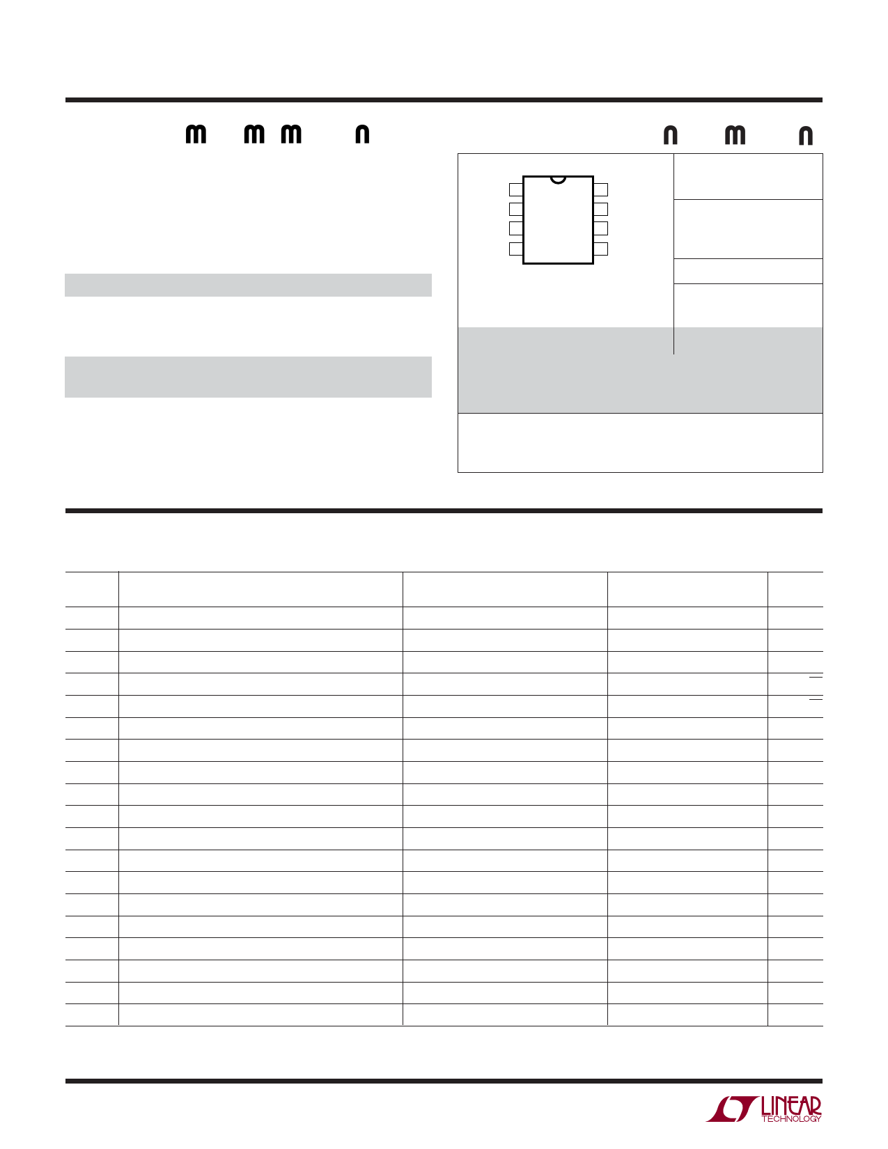
PACKAGE/ORDER I FOR ATIO
TOP VIEW
NULL 1
–IN 2
+IN 3
V– 4
8 SHUTDOWN
7 V+
6 OUT
5 NULL
N8 PACKAGE
S8 PACKAGE
8-LEAD PLASTIC DIP 8-LEAD PLASTIC SO
TJ MAX = 150°C, θJA = 100°C/W(N8)
TJ MAX = 150°C, θJA = 150°C/W(S8)
ORDER PART
NUMBER
LT1223CN8
LT1223CS8
S8 PART MARKING
1223
J8 PACKAGE
8-LEAD CERAMIC DIP
TJMAX = 175°C, θJA = 100°CW (J8)
LT1223CJ8
LT1223MJ8
OBSOLETE PACKAGE
Consider the N8 or S8 for Alternative Source
Order Options Tape and Reel: Add #TR
Lead Free: Add #PBF Lead Free Tape and Reel: Add #TRPBF
Lead Free Part Marking: http://www.linear.com/leadfree/
Consult LTC Marketing for parts specified with wider operating temperature ranges.
ELECTRICAL CHARACTERISTICS VS = ± 15V, TA = 25°C, unless otherwise noted.
SYMBOL
VOS
IIN+
IIN–
en
in
RIN
CIN
CMRR
PSRR
AV
ROL
VOUT
IOUT
SR
BW
PARAMETER
Input Offset Voltage
Noninverting Input Current
Inverting Input Current
Input Noise Voltage Density
Input Noise Current Density
Input Resistance
Input Capacitance
Input Voltage Range
Common Mode Rejection Ratio
Inverting Input Current Common Mode Rejection
Power Supply Rejection Ratio
Noninverting Input Current Power Supply Rejection
Inverting Input Current Power Supply Rejection
Large Signal Voltage Gain
Transresistance, ∆VOUT/∆IIN–
Maximum Output Voltage Swing
Maximum Output Current
Slew Rate
Bandwidth
CONDITIONS
VCM = 0V
VCM = 0V
VCM = 0V
f = 1kHz, RF = 1k, RG = 10Ω
f = 1kHz, RF = 1k, RG = 10Ω
VIN = ±10V
VCM = ±10V
VCM = ±10V
VS = ±4.5V to ±18V
VS = ±4.5V to ±18V
VS = ±4.5V to ±18V
RLOAD = 400Ω, VOUT = ±10V
RLOAD = 400Ω, VOUT = ±10V
RLOAD = 200Ω
RLOAD = 200Ω
RF = 1.5k, RG = 1.5k (Note 3)
RF = 1k, RG = 1k, VOUT = 100mV
LT1223M/C
MIN
TYP MAX
±1
±3
±1
±3
±1
±3
3.3
2.2
1
10
1.5
± 10
± 12
56
63
30
100
68
80
12
100
60
500
70
89
1.5
5
± 10
± 12
50
60
800
1300
100
UNITS
mV
µA
µA
nV/√Hz
pA/√Hz
MΩ
pF
V
dB
nA / V
dB
nA / V
nA / V
dB
MΩ
V
mA
V/µs
MHz
1223fb
2
Share Link: 