LT1228(Rev_A) 查看數據表(PDF) - Linear Technology
零件编号
产品描述 (功能)
生产厂家
LT1228 Datasheet PDF : 20 Pages
| |||
LT1228
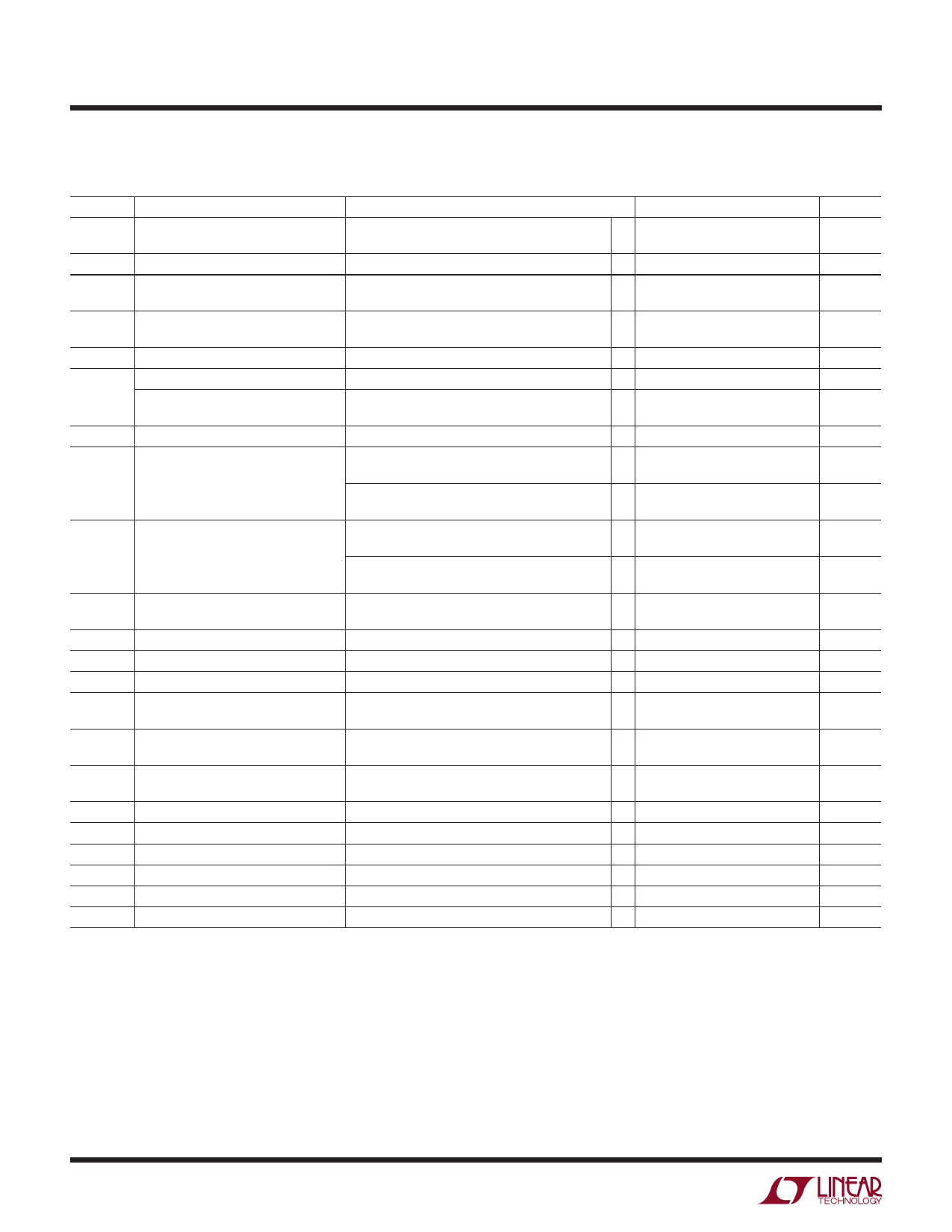
ELECTRICAL CHARACTERISTICS
Transconductance Amplifier, Pins 1, 2, 3, 5. ±5V ≤ VS ≤ ±15V, ISET = 100µA, VCM = 0V unless otherwise noted.
SYMBOL PARAMETER
CONDITIONS
MIN TYP MAX UNITS
CMRR
Common-Mode Rejection Ratio
PSRR
gm
Power Supply Rejection Ratio
Transconductance
Transconductance Drift
VS = ±15V, VCM = ±13V, TA = 25°C
VS = ±15V, VCM = ±12V
VS = ±5V, VCM = ±3V, TA = 25°C
VS = ±5V, VCM = ±2V
VS = ±2V to ±15V, TA = 25°C
VS = ±3V to ±15V
ISET = 100µA, IOUT = ±30µA, TA = 25°C
60 100
dB
q 60
dB
60 100
dB
q 60
dB
60 100
dB
q 60
dB
0.75 1.00 1.25 µA/mV
q
– 0.33
%/°C
IOUT
Maximum Output Current
IOL
Output Leakage Current
ISET = 100µA
ISET = 0µA (+IIN of CFA), TA = 25°C
q 70 100 130
µA
0.3 3
µA
q
10
µA
VOUT
Maximum Output Voltage Swing
RO
Output Resistance
Output Capacitance (Note 2)
IS
Supply Current, Both Amps
THD
Total Harmonic Distortion
BW
Small-Signal Bandwidth
tr
Small-Signal Rise Time
Propagation Delay
VS = ±15V , R1 = ∞
VS = ±5V , R1 = ∞
VS = ±15V, VOUT = ±13V
VS = ±5V, VOUT = ±3V
VS = ±5V
ISET = 1mA
VIN = 30mVRMS at 1kHz, R1 = 100k
R1 = 50Ω, ISET = 500µA
R1 = 50Ω, ISET = 500µA, 10% to 90%
R1 = 50Ω, ISET = 500µA, 50% to 50%
q ±13 ±14
V
q ±3 ±4
V
q2
8
MΩ
q2
8
MΩ
6
pF
q
9
15
mA
0.2
%
80
MHz
5
ns
5
ns
The q denotes specifications which apply over the operating temperature
range.
Note 1: A heat sink may be required depending on the power supply
voltage.
Note 2: This is the total capacitance at pin 1. It includes the input
capacitance of the current feedback amplifier and the output capacitance
of the transconductance amplifier.
Note 3: Slew rate is measured at ±5V on a ±10V output signal while
operating on ±15V supplies with RF = 1k, RG = 110Ω and RL = 400Ω. The
slew rate is much higher when the input is overdriven, see the applications
section.
Note 4: Rise time is measured from 10% to 90% on a ±500mV output
signal while operating on ±15V supplies with RF = 1k, RG = 110Ω and
RL = 100Ω. This condition is not the fastest possible, however, it does
guarantee the internal capacitances are correct and it makes automatic
testing practical.
Note 5: AC parameters are 100% tested on the ceramic and plastic DIP
packaged parts (J and N suffix) and are sample tested on every lot of
the SO packaged parts (S suffix).
Note 6: NTSC composite video with an output level of 2V.
Note 7: Back to back 6V Zener diodes are connected between pins 2 and
3 for ESD protection.
4
Share Link: 