LT1228CS8 查看數據表(PDF) - Linear Technology
零件编号
产品描述 (功能)
生产厂家
LT1228CS8 Datasheet PDF : 22 Pages
| |||
LT1228
ABSOLUTE MAXIMUM RATINGS
(Note 1)
Supply Voltage........................................................ ±18V
Input Current, Pins 1, 2, 3, 5, 8 (Note 8)...............±15mA
Output Short Circuit Duration (Note 2).......... Continuous
Operating Temperature Range
LT1228C....................................................0°C to 70°C
LT1228I.................................................–40°C to 85°C
LT1228M (OBSOLETE)....................... –55°C to 125°C
Storage Temperature Range................... –65°C to 150°C
Junction Temperature
Plastic Package.................................................. 150°C
Ceramic Package (OBSOLETE).......................... 175°C
Lead Temperature (Soldering, 10 sec)....................300°C
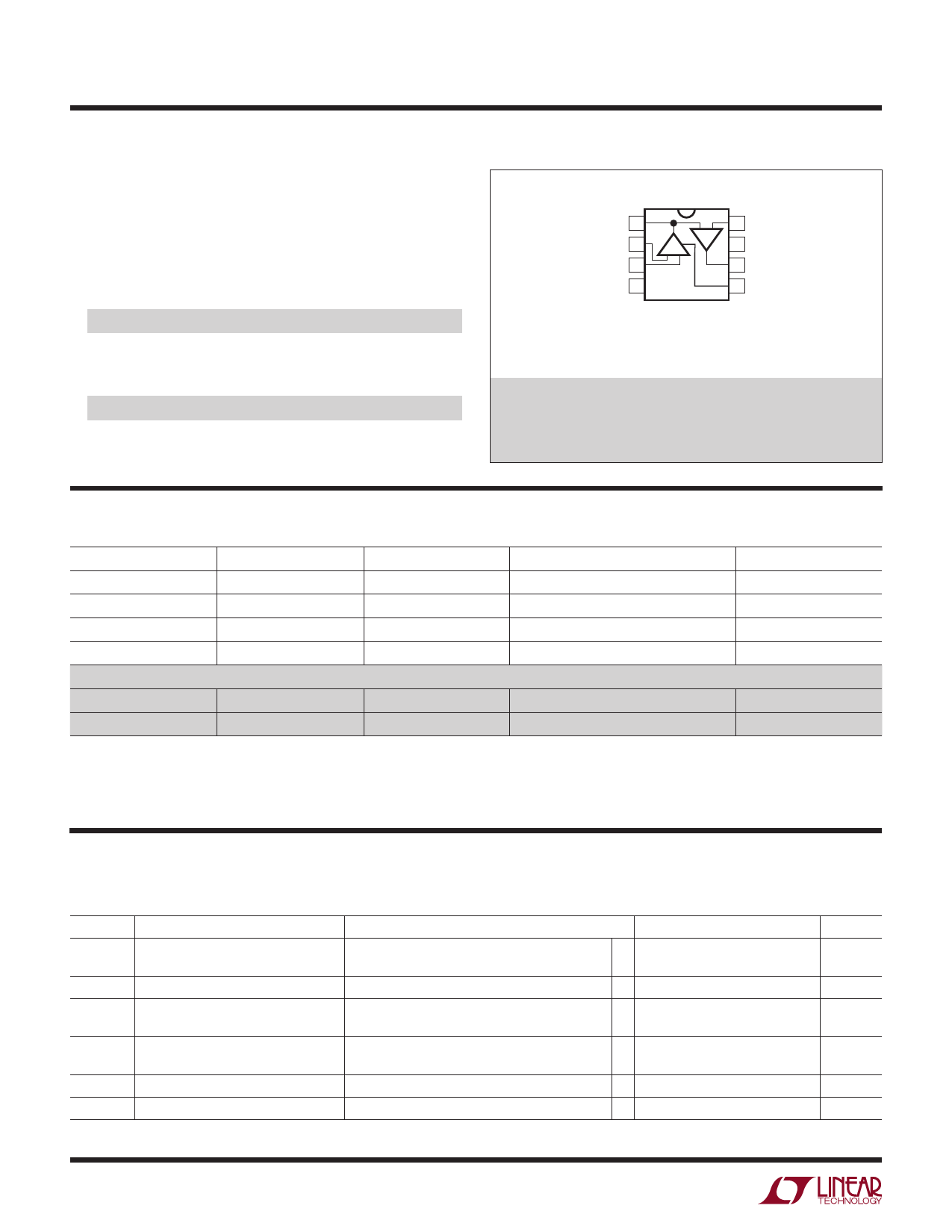
PIN CONFIGURATION
TOP VIEW
IOUT 1
–IN 2
+IN 3
V– 4
+–
gm
8 GAIN
7 V+
6 VOUT
5 ISET
N8 PACKAGE
8-LEAD PDIP
S8 PACKAGE
8-LEAD PLASTIC SO
TJMAX = 150°C, θJA = 100°C/W (N)
TJMAX = 150°C, θJA = 150°C/W (N)
J8 PACKAGE
8-LEAD CERDIP
TJMAX = 175°C, θJA = 100°C/W (J)
OBSOLETE PACKAGE
ORDER INFORMATION
LEAD FREE FINISH
TAPE AND REEL
PART MARKING
PACKAGE DESCRIPTION
LT1228CN8#PBF
LT1228CN8#TRPBF
LT1228CN8
8-Lead Plastic DIP
LT1228IN8#PBF
LT1228IN8#TRPBF
LT1228IN8
8-Lead Plastic DIP
LT1228CS8#PBF
LT1228CS8#TRPBF
1228
8-Lead Plastic SO
LT1228IS8#PBF
LT1228IS8#TRPBF
1228I
8-Lead Plastic SO
OBSOLETE PACKAGE
LT1228MJ8
LT1228MJ8#TRPBF
LT1228MJ8
8-Lead CERDIP
LT1228CJ8
LT1228CJ8#TRPBF
LT1228CJ8
8-Lead CERDIP
Consult LTC Marketing for parts specified with wider operating temperature ranges.
Consult LTC Marketing for information on nonstandard lead based finish parts.
For more information on lead free part marking, go to: http://www.linear.com/leadfree/
For more information on tape and reel specifications, go to: http://www.linear.com/tapeandreel/
TEMPERATURE RANGE
0°C to 70°C
–40°C to 85°C
0°C to 70°C
–40°C to 85°C
–55°C to 125°C
0°C to 70°C
ELECTRICAL CHARACTERISTICS The l denotes the specifications which apply over the full operating
temperature range, otherwise specifications are at TA = 25°C. Current Feedback Amplifier, Pins 1, 6, 8. ±5V ≤ VS ≤ ±15V, ISET = 0µA,
VCM = 0V unless otherwise noted.
SYMBOL PARAMETER
CONDITIONS
MIN
TYP
MAX
UNITS
VOS
Input Offset Voltage
TA = 25°C
±3
±10
mV
l
±15
mV
Input Offset Voltage Drift
l
10
µV/°C
IIN+
Noninverting Input Current
TA = 25°C
±0.3
±3
µA
l
±10
µA
IIN–
Inverting Input Current
TA = 25°C
±10
±65
µA
l
±100
µA
en
Input Noise Voltage Density
in
Input Noise Current Density
f = 1kHz, RF = 1k, RG = 10Ω, RS = 0Ω
f = 1kHz, RF = 1k, RG = 10Ω, RS = 10k
6
nV/√Hz
1.4
pV/√Hz
1228fd
2
Share Link: 