ADP667AN 查看數據表(PDF) - Analog Devices
零件编号
产品描述 (功能)
生产厂家
ADP667AN Datasheet PDF : 8 Pages
| |||
ADP667
Dropout Detector
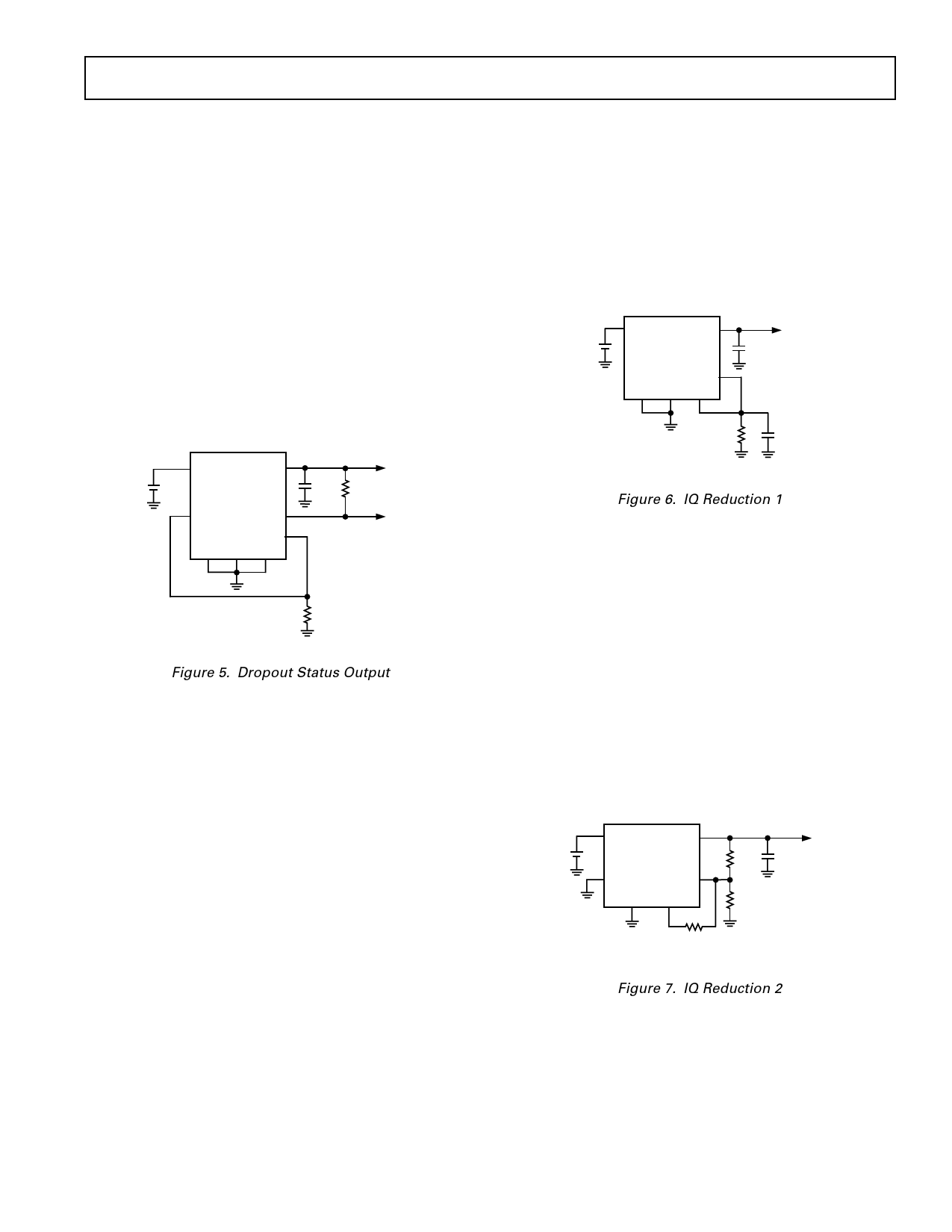
The ADP667 features an extremely low dropout voltage making
it suitable for low voltage systems where headroom is limited. A
dropout detector is also provided. The dropout detector output,
DD, changes as the dropout voltage approaches its limit. This is
useful for warning that regulation can no longer be maintained.
The dropout detector output is an open collector output from a
PNP transistor. Under normal operating conditions with the in-
put voltage more than 300 mV above the output, the PNP tran-
sistor is off and no current flows out the DD pin. As the voltage
differential reduces to less than 300 mV, the transistor switches
on and current is sourced. This condition indicates that regulation
can no longer be maintained. Please refer to Figure 10 in the
“Typical Performance Characteristics.” The current output can
be translated into a voltage output by connecting a resistor from
DD to GND. A resistor value of 100 kΩ is suitable. A digital
status signal can be obtained using a comparator. The on-chip
comparator LBI may be used if it is not being used to monitor a
battery voltage. This is illustrated in Figure 5.
+
VIN
IN
OUT
ADP667
+ C1
10µF
R2
10kΩ
+5V
OUTPUT
LBI
LBO
DD
SET GND SHDN
DROPOUT
STATUS
OUTPUT
R1
100kΩ
Figure 5. Dropout Status Output
Output Capacitor Selection
An output capacitor is required on the ADP667 to maintain
stability and also to improve the load transient response. Ca-
pacitor values from 10 µF upwards are suitable. All specifica-
tions are tested and guaranteed with 10 µF. Capacitors larger
than 10 µF will further improve the dynamic transient response
characteristics of the regulator. Tantalum or aluminum electro-
lytics are suitable for most applications. For temperatures below
about –25°C, solid tantalums should be used as many alumi-
num electrolytes freeze at this temperature.
Quiescent Current Considerations
The ADP667 uses a PNP output stage to achieve low dropout
voltages combined with high output current capability. Under
normal regulating conditions the quiescent current is extremely
low. However if the input voltage drops so that it is below the
desired output voltage, the quiescent current increases consider-
ably. This happens because regulation can no longer be main-
tained and large base current flows in the PNP output transistor
in an attempt to hold it fully on. For minimum quiescent cur-
rent, it is therefore important that the input voltage is main-
tained higher than the desired output level. If the device is being
powered using a battery that can discharge down below the rec-
ommended level, there are a couple of techniques that can be
applied to reduce the quiescent current, but at the expense of
dropout voltage. The first of these is illustrated in Figure 6. By
connecting DD to SHDN the regulator is partially disabled with
input voltages below the desired output voltage and therefore
the quiescent current is reduced considerably.
+
VIN
IN
OUT
ADP667
DD
SET GND SHDN
+ C1
10µF
+5V
OUTPUT
R1
47kΩ
C2
0.1µF
Figure 6. IQ Reduction 1
Another technique for reducing the quiescent current near drop-
out is illustrated in Figure 7. The DD output is used to modify
the output voltage so that as VIN drops, the desired output volt-
age setpoint also drops. This technique only works when exter-
nal resistors are used to set the output voltage. With VIN greater
than VOUT, DD has no effect. As VIN reduces and dropout is
reached, the DD output starts sourcing current into the SET
input through R3. This increases the SET voltage so that the
regulator feedback loop does not drive the internal PNP transis-
tor as hard as it otherwise would. As the input voltage continues
to decrease, more current is sourced, thereby reducing the PNP
drive even further. The advantage of this scheme is that it main-
tains a low quiescent current down to very low values of VIN at
which point the batteries are well outside their useful operating
range. The output voltage tracks the input voltage minus the
dropout. The SHDN function is also unaffected and may be
used normally if desired.
+
VIN
IN
OUT
ADP667
SHDN
SET
GND DD
R3
1MΩ
R2
1MΩ
+ C1
10µF
+5V
OUTPUT
R1
332kΩ
Figure 7. IQ Reduction 2
REV. 0
–5–
Share Link: 