5962-89839072A 查看數據表(PDF) - Lattice Semiconductor
零件编号
产品描述 (功能)
生产厂家
5962-89839072A Datasheet PDF : 8 Pages
| |||
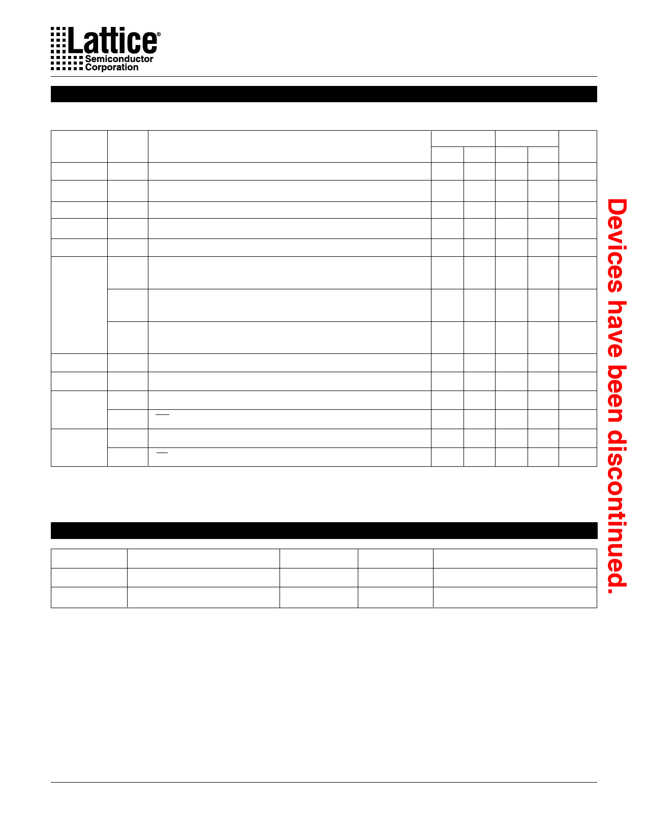
Specifications GAL16V8D-7/10/883
AC Switching Characteristics
Over Recommended Operating Conditions
TEST
PARAMETER COND1.
DESCRIPTION
tpd
A
Input or I/O to Combinational Output
tco
A
Clock to Output Delay
tcf2
— Clock to Feedback Delay
tsu
— Setup Time, Input or Feedback before Clock↑
th
— Hold Time, Input or Feedback after Clock↑
A
Maximum Clock Frequency with
External Feedback, 1/(tsu + tco)
fmax3
A
Maximum Clock Frequency with
Internal Feedback, 1/(tsu + tcf)
A
Maximum Clock Frequency with
No Feedback
twh
— Clock Pulse Duration, High
twl
— Clock Pulse Duration, Low
ten
B
Input or I/O to Output Enabled
B
OE to Output Enabled
tdis
C
Input or I/O to Output Disabled
C
OE to Output Disabled
-7
MIN. MAX.
1 7.5
-10
MIN. MAX.
2 10
UNITS
ns
1
6
1
7
ns
—6—7
ns
7
— 10 —
ns
0
—
0
—
76.9 — 58.8 —
ns
MHz
76.9 — 58.8 — MHz
100 — 62.5 — MHz
5
—
8
—
ns
5
—
8
—
ns
1
9
— 10
ns
1
7
— 10
ns
1
9
— 10
ns
1
7
— 10
ns
1) Refer to Switching Test Conditions section.
2) Calculated from fmax with internal feedback. Refer to fmax Descriptions section.
3) Refer to fmax Descriptions section.
Capacitance (TA = 25°C, f = 1.0 MHz)
SYMBOL
PARAMETER
CI
Input Capacitance
CI/O
I/O Capacitance
*Characterized but not 100% tested.
MAXIMUM*
10
10
UNITS
pF
pF
TEST CONDITIONS
VCC = 5.0V, VI = 2.0V
VCC = 5.0V, VI/O = 2.0V
3
Share Link: 