FAN5071 查看數據表(PDF) - Fairchild Semiconductor
零件编号
产品描述 (功能)
生产厂家
FAN5071
Fairchild Semiconductor

FAN5071 Datasheet PDF : 15 Pages
| |||
FAN5071
Start and current limiting. The linears start instantly, not
waiting for softstart. The FAN5071 is available in a 24 pin
SOIC package.
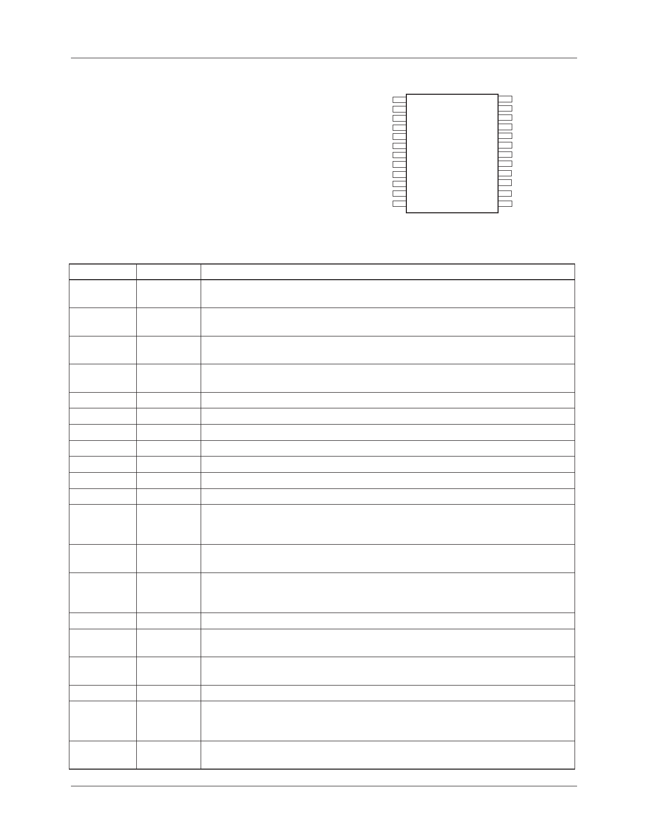
Pin Assignments
HIDRV
SW
GNDA
VID4
VID3
VID2
VID1
VID0
VADJGATE
VADJFB
VCKGATE
VCKFB
1
24
2
23
3
22
4
21
5
20
6
FAN5071 19
7
18
8
17
9
16
10
15
11
14
12
13
VCCP
LODRV
GNDP
VCCA
VFB
DROOP
ILIM
PWRGD
SS/ENABLE
TYPEDET
VAGPGATE
VAGPFB
Pin Definitions
Pin Number Pin Name
Pin Function Description
1
HIDRV High Side FET Driver. Connect this pin to the gate of an N-channel MOSFET. The
trace from this pin to the MOSFET gate should be <0.5".
2
SW
High Side Driver Source and Low Side Driver Drain Switching Node. Together
with DROOP and ILIM pins allows FET sensing for VCC current.
3
GNDA Analog Ground. Return path for low power analog circuitry. This pin should be
connected to a low impedance system ground plane to minimize ground loops.
4-8
VID4-0 Voltage Identification Code Inputs. These open collector/TTL compatible inputs
will program the output voltage over the ranges specified in Table 1.
9
VADJGATE Gate Driver for VADJ Transistor. For Adjustable output.
10
VADJFB Voltage Feedback for VADJ.
11
VCKGATE Gate Driver for VCK Transistor. For 2.5V output.
12
VCKFB Voltage Feedback for VCK.
13
VAGPFB Voltage Feedback for VAGP.
14
VAGPGATE Gate Driver for VAGP Transistor. For 3.3/1.5V output.
15
TYPEDET Type Detect. Sets 3.3V or 1.5V for AGP.
16
ENABLE/SS Output Enable. A logic LOW on this pin will disable all outputs. An internal current
source allows for open collector control. This pin also doubles as soft start for the
switcher.
17
PWRGD Power Good Flag. An open collector output that will be logic LOW if any output
voltage is not within ±14% of the nominal output voltage setpoint.
18
ILIM
VCC Current Feedback. Pin 18 is used in conjunction with pin 2 as the input for the
VCC current feedback control loop. Layout of these traces is critical to system
performance. See Application Information for details.
19
DROOP Droop Set. Use this pin to set magnitude of active droop.
20
VFB
Vcc Voltage Feedback. Pin 20 is used as the input for the VCC voltage feedback
control loop. See Application Information for details regarding correct layout.
21
VCCA Analog VCC. Connect to system 5V supply and decouple with a 0.1µF ceramic
capacitor.
22
GNDP Power Ground. Return pin for high currents flowing in pin 24 (VCCP).
23
LODRV VCC Low Side FET Driver. Connect this pin to the gate of an N-channel MOSFET
for synchronous operation. The trace from this pin to the MOSFET gate should be
<0.5".
24
VCCP Power VCC. For all FET drivers. Connect to system 12V supply through a 33Ω, and
decouple with a 1µF ceramic capacitor.
2
REV. 1.0.4 1/29/02
Share Link: