MSK101B 查看數據表(PDF) - M.S. Kennedy
零件编号
产品描述 (功能)
生产厂家
MSK101B Datasheet PDF : 6 Pages
| |||
APPLICATION NOTES
CURRENT LIMIT (SEE TYPICAL CONNECTION DIAGRAM)
A value of current limit resistance can be calculated as fol-
lows:
RCL=(0.83 - (0.05 * ICL)) / ICL
Where:
RCL is the current limit resistor value
ICL is the current limit
0.05 * ICL is the voltage dropped in the current limit path
across internal impedances other than the actual current
limit resistor
0.83 volts is the voltage drop that must be developed across
the current limit connections to activate the current limit
circuit
The maximum practical value of current limit resistance is 16
ohms. The current limit resistor will decrease available output
voltage swing in the following manner:
VR=IO * RCL
VR is the reduction in output voltage swing due to the current
limit resistor. It is recommended the user limit output current
to a value as close to the required output current as possible,
without clipping output voltage swing. Current limit will vary
with case temperature. Refer to the typical performance curves
to predict current limit drift. If current limit is not required
replace the resistor with a short.
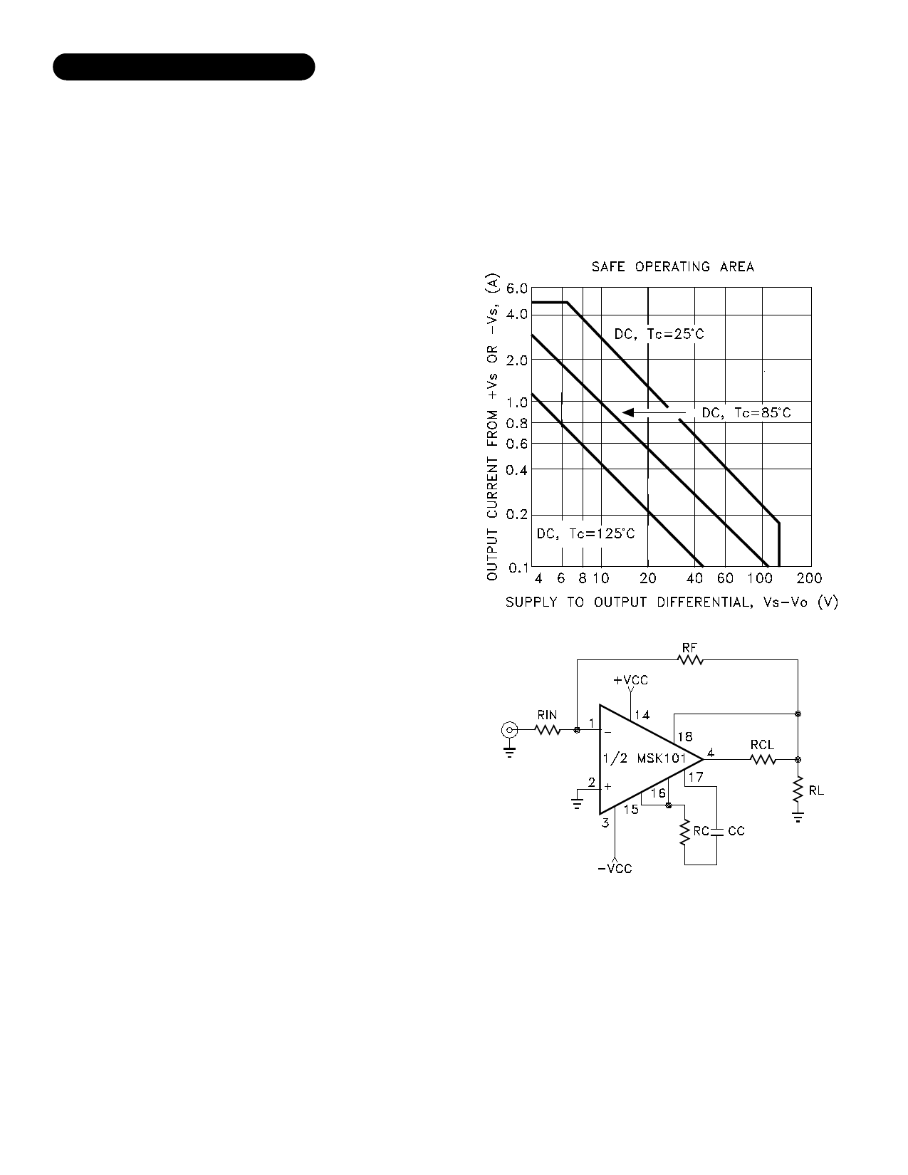
SAFE OPERATING AREA (SOA)
The MOSFET output stage of this power operational ampli-
fier has two distinct limitations:
1. The current handling capability of the die metallization.
2. The junction temperature of the output MOSFET's.
NOTE: The output stage is protected against transient flyback.
However, for protection against sustained, high energy flyback,
external fast-recovery reverse biased diodes should be connected
from the output to ground.
STABILITY
The MSK 101 has sufficient phase margin when compen-
sated for unity gain to be stable with capacitive loads of at
least 10nF. However, it is recommended that the parallel sum
of the input and feedback resistor be 1000 ohms or less for
closed loop gains of ten or less to minimize phase shift caused
by the R-C network formed by the input resistor, feedback re-
sistor and input capacitance. The user can tailor the perfor-
mance of the MSK 101 to their application using the external
compensation pins. The graphs of small signal gain and phase
as well as the graphs of slew rate and power response demon-
strate the effect of various forms of compensation. The com-
pensation capacitor must be rated at 150 volts working voltage
if maximum power supply voltages are used. The compensa-
tion resistor and capacitor lead lengths must be kept as short
as possible to minimize spurious oscillations. A high quality
NPO capacitor is recommended for the compensation capaci-
tor. An effective method of checking amplifier stability is to
apply the worst case capacitive load to the output of the ampli-
fier and drive a small signal square wave across it. If overshoot
is less than 25%, the system will typically be stable.
INPUT PROTECTION
Input protection circuitry within the MSK 101 will clip differ-
ential input voltages greater than 16 volts. The inputs are also
protected against common mode voltages up to the supply rails
as well as static discharge. There are 300 ohm current limiting
resistors in series with each input. These resistors may be-
come damaged in the event the input overload is capable of
driving currents above 1mA. If severe overload conditions are
expected, external input current limiting resistors are recom-
mended.
TYPICAL CONNECTION DIAGRAM
CLASS "C" MODE
The user can enable class "C" mode by simply connecting pin
15 to pin 16 and pin 6 to pin 7. This connection will disable the
bias control network in the output stage of each amplifier.
Quiescent current will drop to ± 8 mA total typically and a
small amount of crossover distortion will appear on the output
waveforms. This mode of operation is recommended for switch-
ing type applications where distortion is not a critical specifica-
tion and quiescent power dissipation must be minimized. Dis-
connecting the pin 15 to pin 16 and pin 6 to pin 7 shorts will
enable the bias control network and the outputs will be biased
in class AB mode again. Pins 15 and 6 should be left uncon-
nected when using class AB mode. (Do not ground or pull high).
3
Rev. A 7/00
Share Link: 