MCM69L817ZP7R 查看數據表(PDF) - Signal Processing Technologies
零件编号
产品描述 (功能)
生产厂家
MCM69L817ZP7R
Signal Processing Technologies

MCM69L817ZP7R Datasheet PDF : 12 Pages
| |||
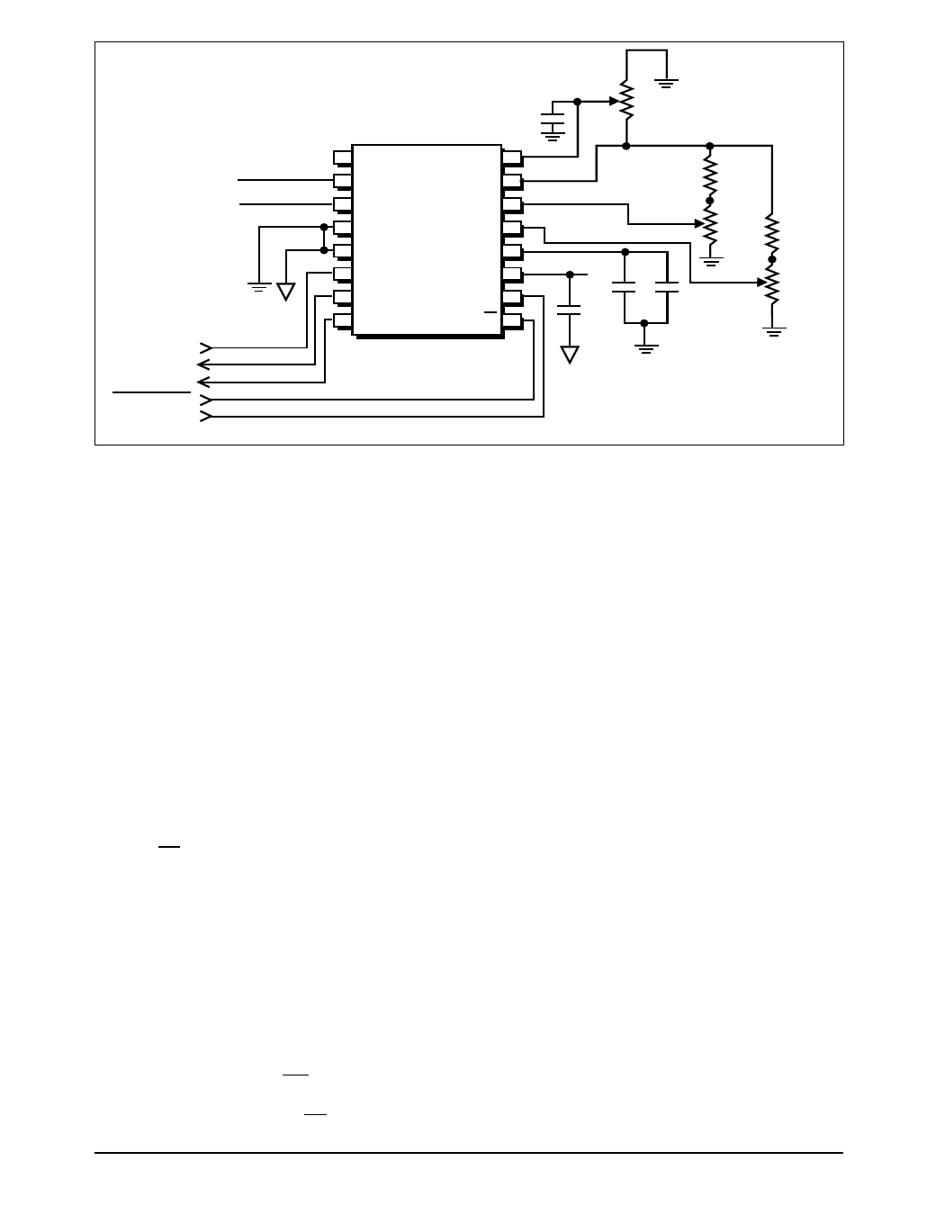
0.01µF*
10kOhms
1 N.C.
GAIN ADJUST 16
VB
2 VIN B
REF OUT 15
VA
3 VIN A OFFSET ADJ. B 14
4 AGND OFFSET ADJ. A 13
5 VSS SP8530 VDA 12
6 SCLK
VDD 11
+5V
7 DOUT
8 STATUS
SHUTDOWN 10
CS 9
0.1µF 6.8µF
0.1µF
CLOCK IN
DATA OUT
STATUS OUT
CHIP SELECT
SHUTDOWN
* Optional filter capacitor is helpful in a noisy pc board application.
Figure 1. Operating Circuit
5kOhms
2kOhms 5kOhms
2kOhms
The device responds to the shut down signal
asynchronously so that a conversion in progress
will be interrupted and the resulting data will be
erroneous. A 20 µSec delay is required between
the falling edge of power down and initiation of
a conversion.
Data Format
32 bits of data are sent for each conversion. The
first 16 bits are the conversion A result, which is
shipped with 4 leading "0"s, and then 12 bits of
data, MSB first. The second 16 bits are the
conversion B result, which are also shipped with
4 leading "0"s, and then 12 bits of data, MSB
first. Data changes on the falling edge of SCLK
and is stable on the rising edge of SCLK.
Continuous stand alone operation is obtained by
holding CS low. In this mode an oscillator is
connected directly to SCLK pin. The SCLK
signal along with the STATUS output Signal
are used to synchronize the host system with the
converter's data. In this mode there is a single
dead SCLK cycle between the 32nd clock of one
conversion and the first clock of the following
conversion for the SP8530. A clock frequency
of 4 MHz the SP8530 provides a throughput
rate of 121KHz.
In slave mode operation, CS is brought high on
each conversion so that all conversions are
initiated by falling edge on CS.
Layout Considerations
Because of the high resolution and linearity of
the SP8530 system design considerations such
as ground path impedance and contact
resistance become very important.
To avoid introducing distortion when driving
the analog inputs of these devices, the source
resistance must be very low, or constant with
signal level. Note that in the operating circuit
there is no connection made between VDA (Pin
12) and the system power supply. This is
because the analog supply pin (VDA) is
connected internally to the digital supply pin
(VDD) through a ten ohm resistor.
This connection when combined with parallel
combination of 6.8µF tantalum and 0.1µF
ceramic capacitor between VDA and analog
ground, will provide some immunity to noise
which resides on the system supply. To maintain
maximum system accuracy, the supply
connected to the VDD pin should be well
isolated from digital supplies and wide load
variations.
To limit effects of digital switching elsewhere
in a system, it often makes sense to run a
separate +5V supply conductor from the supply
regulator to any analog components requiring
+5V including the SP8530. Noise on the power
SP8530DS/01
SP8530 S2ADCTM - Simultaneous Sampling Analog to Digital Converter
6
© Copyright 2000 Sipex Corporation
Share Link: