1SMBXXCAT3 查看數據表(PDF) - ON Semiconductor
零件编号
产品描述 (功能)
生产厂家
1SMBXXCAT3 Datasheet PDF : 6 Pages
| |||
1SMB10CAT3 Series
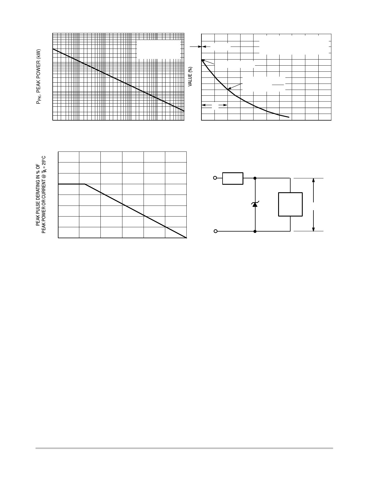
100
NONREPETITIVE
PULSE WAVEFORM
SHOWN IN FIGURE 2
tr ≤ 10 ms
PULSE WIDTH (tP) IS DEFINED
AS THAT POINT WHERE THE PEAK
CURRENT DECAYS TO 50% OF IPP.
100
10
PEAK VALUE − IPP
1
0.1
0.1 ms
160
140
120
100
80
60
40
20
0
0
1 ms
10 ms
100 ms
1 ms
tP, PULSE WIDTH
Figure 1. Pulse Rating Curve
50
HALF VALUE −
IPP
2
0
10 ms
0
tP
1
2
3
4
t, TIME (ms)
Figure 2. Pulse Waveform
TYPICAL PROTECTION CIRCUIT
Zin
Vin
LOAD
VL
25
50
75
100
125
150
TA, AMBIENT TEMPERATURE (°C)
Figure 3. Pulse Derating Curve
APPLICATION NOTES
RESPONSE TIME
In most applications, the transient suppressor device is
placed in parallel with the equipment or component to be
protected. In this situation, there is a time delay associated
with the capacitance of the device and an overshoot
condition associated with the inductance of the device and
the inductance of the connection method. The capacitive
effect is of minor importance in the parallel protection
scheme because it only produces a time delay in the
transition from the operating voltage to the clamp voltage as
shown in Figure 4.
The inductive effects in the device are due to actual
turn-on time (time required for the device to go from zero
current to full current) and lead inductance. This inductive
effect produces an overshoot in the voltage across the
equipment or component being protected as shown in
Figure 5. Minimizing this overshoot is very important in the
application, since the main purpose for adding a transient
suppressor is to clamp voltage spikes. The SMB series have
a very good response time, typically < 1 ns and negligible
inductance. However, external inductive effects could
produce unacceptable overshoot. Proper circuit layout,
minimum lead lengths and placing the suppressor device as
close as possible to the equipment or components to be
protected will minimize this overshoot.
Some input impedance represented by Zin is essential to
prevent overstress of the protection device. This impedance
should be as high as possible, without restricting the circuit
operation.
DUTY CYCLE DERATING
The data of Figure 1 applies for non-repetitive conditions
and at a lead temperature of 25°C. If the duty cycle increases,
the peak power must be reduced as indicated by the curves
of Figure 6. Average power must be derated as the lead or
ambient temperature rises above 25°C. The average power
derating curve normally given on data sheets may be
normalized and used for this purpose.
At first glance the derating curves of Figure 6 appear to be
in error as the 10 ms pulse has a higher derating factor than
the 10 ms pulse. However, when the derating factor for a
given pulse of Figure 6 is multiplied by the peak power value
of Figure 1 for the same pulse, the results follow the
expected trend.
http://onsemi.com
4
Share Link: 