HT604L 查看數據表(PDF) - Holtek Semiconductor
零件编号
产品描述 (功能)
生产厂家
HT604L Datasheet PDF : 12 Pages
| |||
HT604L/HT614/HT692
Functional Description
Operation
The 318 series of decoders provide various combina-
tions of address and data pins in different packages. It is
paired with the 318 series of encoders. The decoders re-
ceive data transmitted by the encoders and interpret the
first N bits of the code period as address and the last
18-N bits as data (where N is the address code num-
ber). A signal on the DIN pin then activates the oscillator
which in turns decodes the incoming address and data.
The decoders will check the received address twice
continuously. If all the received address codes match
the contents of the decoder¢s local address, the 18-N
bits of data are decoded to activate the output pins, and
the VT pin is set high to indicate a valid transmission.
That will last until the address code is incorrect or no sig-
nal has been received. The output of the VT pin is high
only when the transmission is valid. Otherwise it is al-
ways low.
Output Type
There are two types of output to select from:
· Momentary type
The data outputs follow the encoder during a valid
transmission and then reset.
· Latch type
The data outputs follow the encoder during a valid
transmission, and are then latched in this state until
the next valid transmission occurs.
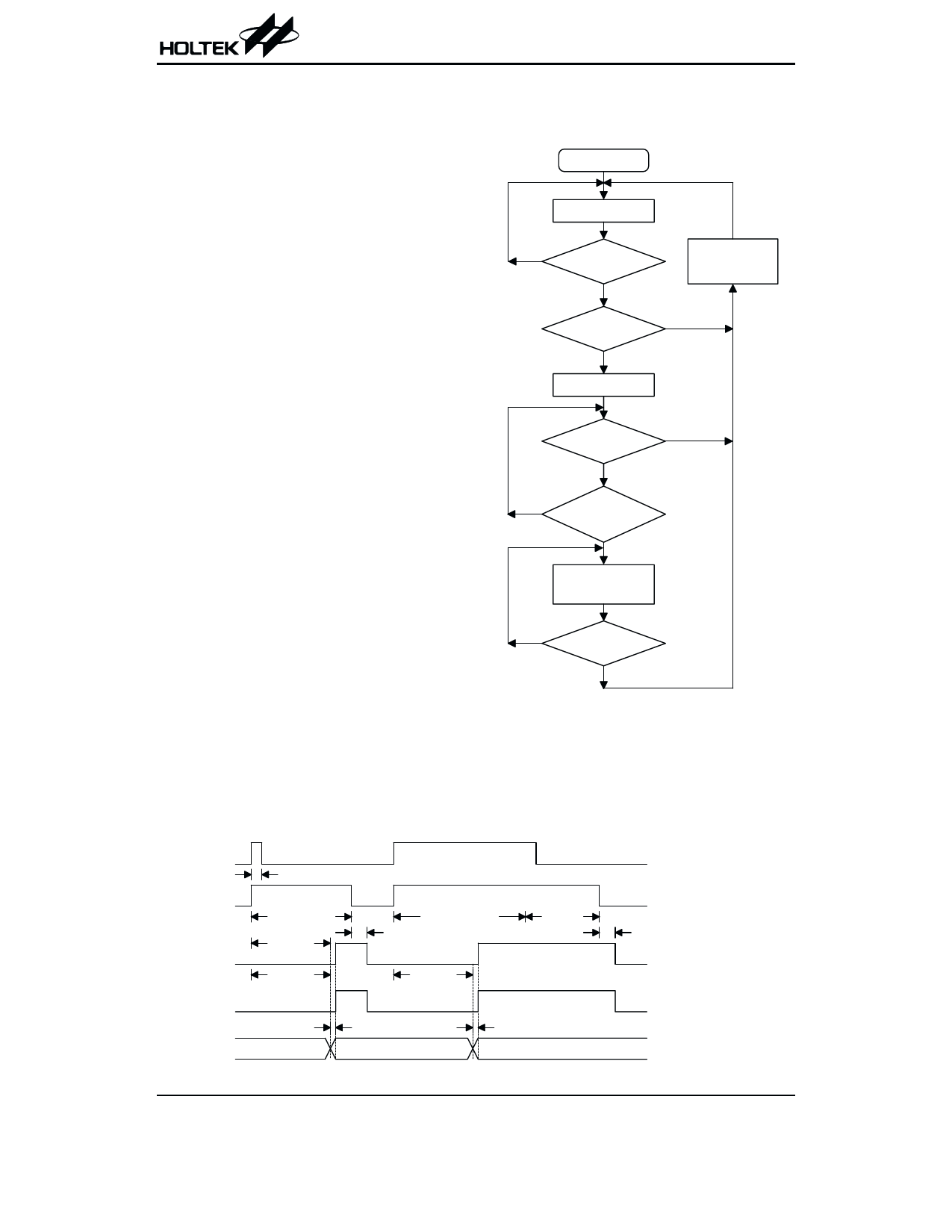
Flowchart
P ow eron
S ta n d b y m o d e
No
C o d e in ?
Y es
D is a b le V T &
ig n o r e th e r e s t o f
th is w o r d
A d d r e s s b its
No
m a tc h e d ?
Y es
S to re d a ta
M a tc h
p r e v io u s s to r e d
No
d a ta ?
Y es
No
2 tim e s
o f c h e c k in g
c o m p le te d ?
Y es
L a tc h /M o m e n ta ry
d a ta to o u tp u t &
a c tiv a te V T
No
A d d re s s o r
d a ta e rro r ?
Y es
Note: The oscillator is disabled in the standby state
and activated as long as a logic ²high² signal
is applied to the DIN pin. i.e., the DIN should
be kept ²low² if there is no signal input.
Decoder timing
E ncoder
T r a n s m is s io n
E n a b le
E ncoder
D a ta O u t
D ecoder V T
M o m e n ta ry
D a ta O u t
< 1 w o rd
3 w o rd s
2 w o rd s
check
L a tc h e d
D a ta O u t
Rev. 1.10
T r a n s m itte d
C o n tin u o u s ly
2 1 4 c lo c k s
check
3 w o rd s
1 /2 c lo c k p e r io d
1 /2 c lo c k p e r io d
4
2 1 4 c lo c k s
January 24, 2003
Share Link: 