29C010JI-3 查看數據表(PDF) - Turbo IC Inc
零件编号
产品描述 (功能)
生产厂家
29C010JI-3
Turbo IC Inc

29C010JI-3 Datasheet PDF : 8 Pages
| |||
Turbo IC, Inc.
29C010
ADVANCE INFORMATION
ABSOLUTE MAXIMUM STRESS RANGES *
TEMPERATURE
Storage:
Under Bias:
-65° C to 150° C
-55° C to 125° C
ALL INPUT OR OUTPUT VOLTAGES
with respect to Vss
+6 V to -0.3 V
* “Absolute Maximum Ratings” may cause permanent damage to the de-
vice. This is a stress rating only and functional operation of the device at
these or any other conditions above those indicated in the operation sec-
tion of this specification is not implied. Exposure to absolute maximum
rating conditions for extended periods may affect device reliability.
RECOMMENDED OPERATING CONDITIONS
Temperature Range:
Commercial:
Industrial:
Military:
0° C to 70° C
-40° C to 85° C
-55° C to 125° C
Vcc Supply Voltage:
5 V ± 10%
Endurance:
Data Retention:
10,000 Cycles/Byte (Typical)
10 Years
A.C. CHARACTERISTICS - READ OPERATION
D.C. CHARACTERISTICS
Symbol Parameter Condition
Min
(C) = COMMERCIAL
(I) = INDUSTRIAL
(M) = MILITARY
Max Units
Icc Active Vcc CE=OE=Vil; All I/O
Current
Open, Min Read or
Write Cycle Time
Isb1 CMOS
CE=Vcc-0.3 V to
Standby
Vcc+1 V
Current
Isb2 TTL Standby CE=Vih, OE=Vil,
Current
All I/O Open, Other
Inputs=Vcc Max
60 (C) mA
70 (I) mA
90 (M) mA
100 (C) µA
200 (I&M) µA
3
mA
Iil
Input
Vin=Vcc Max
1
µA
Leakage
Current
Iol Output
10
µA
Leakage
Current
Vil Input Low
-0.1
-0.8
V
Voltage
Vih Input High
2 Vcc+0.3
V
Voltage
Vol Output Low Iol=2.1 mA
0.45
V
Voltage
Voh Output High Ioh=-0.45 mA 2.4
V
Voltage
29C010-1 29C010-2 29C010-3
Symbol Parameters Min Max Min Max Min Max
Unit
tacc
Address to
120
150
200
ns
Output Delay
tce
CE to Output
120
150
200
ns
Delay
toe
OE to Output
70
80
90
ns
tdf
OE to Output 0 40 0 50 0 60
ns
In High Z
toh
Output Hold
0
0
0
ns
from Address
Changes, Chip
Enable or
Output Enable
Whichever
Occurs First
A.C. TEST CONDITIONS
Output Load : 1 TTL Load and Cl=100 pF
Input Rise and Fall Times : < 10 ns
Input Pulse Level : 0.45 V to 2.4V
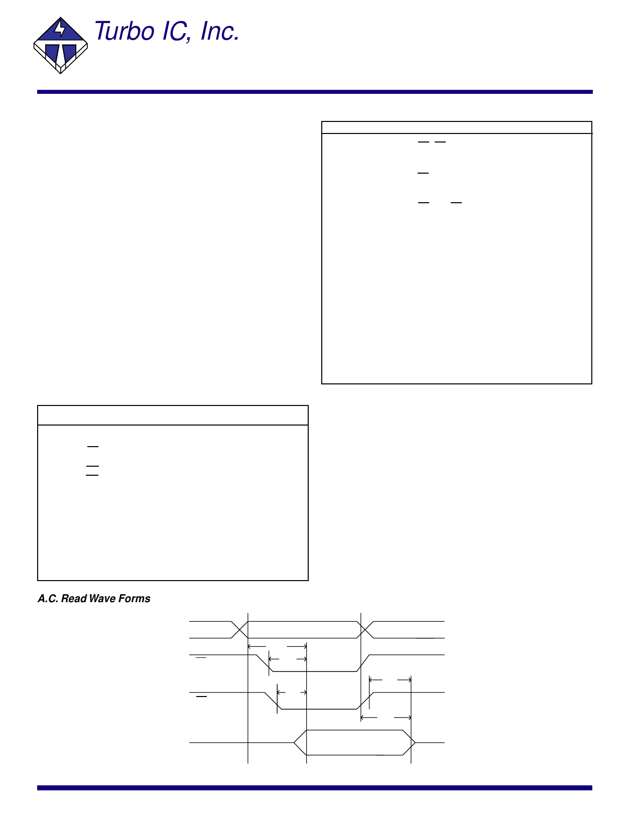
A.C. Read Wave Forms
ADDRESS
CE
OE
OUTPUT
ADDRESS VALID
tacc
tce
tdf
toe
HIGH-Z
toh
OUTPUT VALID
HIGH-Z
Share Link: