MAX477EPA 查看數據表(PDF) - Maxim Integrated
零件编号
产品描述 (功能)
生产厂家
MAX477EPA Datasheet PDF : 12 Pages
| |||
300MHz High-Speed Op Amp
As an example, consider RS = 75Ω, Rf = Rg = 500Ω.
Then:
( ) REQ = 75Ω + 500Ω ||500Ω = 325Ω
eR = 4KT x 325 = 2.3nV / Hz at + 25°C
eT = (5nV)2 + (2.3nV)2 + (2pA x 325)2 = 5.5nV Hz
3) The MAX477’s output-referred noise is simply total
input-referred noise, eT, multiplied by the gain
factor:
e OUT
=
eT
1+
Rf
Rg
In the above example, with eT = 5.5nV√Hz, and assum-
ing a signal bandwidth of 300MHz (471MHz noise
bandwidth), total output noise in this bandwidth is:
e OUT
=
5.5nV x 1 +
500
500
x
471MHz = 239µVRMS
Note that for both DC and noise calculations, errors are
dominated by offset voltage (VOS) and input noise volt-
age (en). For a current-mode feedback amplifier with
offset and noise errors significantly higher, the calcula-
tions are very different.
Driving Capacitive Loads
The MAX477 provides maximum AC performance with
no output load capacitance. This is the case when the
MAX477 is driving a correctly terminated transmission
line (i.e., a back-terminated 75Ω cable). However, the
MAX477 is capable of driving capacitive loads up to
100pF without oscillations, but with reduced AC perfor-
mance.
Driving large capacitive loads increases the chance of
oscillations in most amplifier circuits. This is especially
true for circuits with high loop gain, such as voltage fol-
lowers. The amplifier’s output resistance and the load
capacitor combine to add a pole and excess phase to
the loop response. If the frequency of this pole is low
enough and phase margin is degraded sufficiently,
oscillations may occur.
A second problem when driving capacitive loads
results from the amplifier’s output impedance, which
looks inductive at high frequency. This inductance
forms an L-C resonant circuit with the capacitive load,
which causes peaking in the frequency response and
degrades the amplifier’s gain margin.
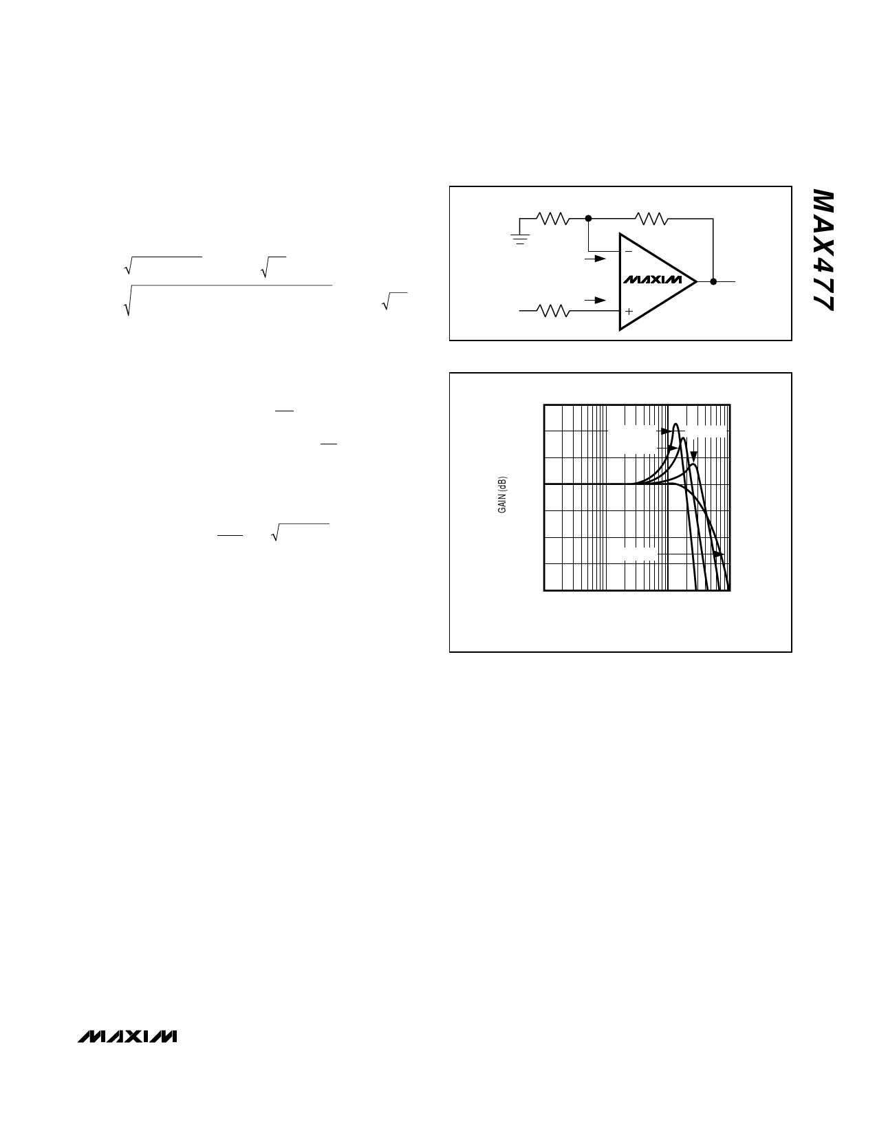
Rg
Rf
IB-
VOUT
RS
MAX477
IB+
VIN
Figure 3. Output Offset Voltage
15
10
5
0
-5
-10
-15
-20
1M
CL = 100pF
CL = 41pF
CL = 22pF
CL = 0pF
10M
100M
1G
FREQUENCY (Hz)
Figure 4. Effect of CLOAD on Frequency Response (AVCL = +1V/V)
The MAX477 drives capacitive loads up to 100pF with-
out oscillation. However, some peaking (in the frequen-
cy domain) or ringing (in the time domain) may occur.
This is shown in Figure 4 and in the Small and Large-
Signal Pulse Response graphs in the Typical Operating
Characteristics.
To drive larger-capacitance loads or to reduce ringing,
add an isolation resistor between the amplifier’s output
and the load, as shown in Figure 5.
The value of RISO depends on the circuit’s gain and the
capacitive load. Figure 6 shows the Bode plots that
result when a 20Ω isolation resistor is used with a volt-
age follower driving a range of capacitive loads. At the
higher capacitor values, the bandwidth is dominated by
the RC network, formed by RISO and CL; the bandwidth
of the amplifier itself is much higher. Note that adding
an isolation resistor degrades gain accuracy. The load
and isolation resistor form a divider that decreases the
voltage delivered to the load.
_______________________________________________________________________________________ 9
Share Link: 