HV430WG 查看數據表(PDF) - Supertex Inc
零件编号
产品描述 (功能)
生产厂家
HV430WG Datasheet PDF : 9 Pages
| |||
Ordering Information
Part Number
Package Option Packing
HV430WG-G
20-Lead SOW 1000/Reel
-G denotes a lead (Pb)-free / RoHS compliant package
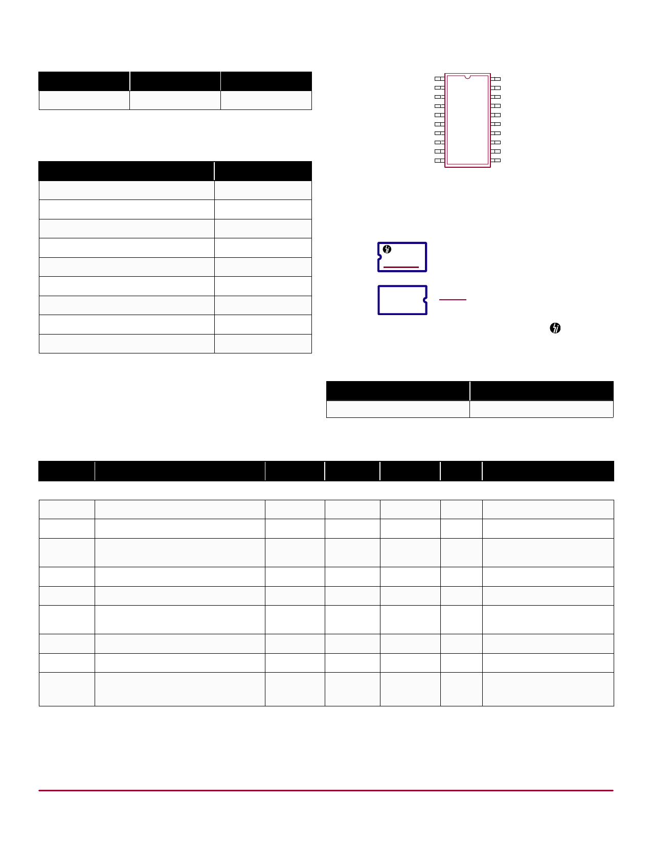
Pin Configuration
1
HV430
20
Absolute Maximum Ratings
Parameter
Value
VPP1 - VNN1, power supply voltage
VPP1, positive high voltage supply
VPP2, positive gate voltage supply
VNN1, negative high voltage supply
VNN2, negative gate voltage supply
VDD, logic supply
Operating temperature range
+340V
+220V
+220V
-220V
-220V
+7.5V
-40OC to +85OC
Storage temperature range
-65OC to +150OC
Power dissipation
600mW
Stresses beyond those listed under “Absolute Maximum Ratings” may
cause permanent damage to the device. These are stress ratings only,
and functional operation of the device at these or any other conditions
beyond those indicated in the operational sections of the specifications is
not implied. Exposure to absolute maximum rating conditions for extended
periods may affect device reliability.
20-Lead SOW
(top view)
Product Marking
Top Marking
YYWW AAA
HV430WG
LLLLLLLLLL
Bottom Marking
CCCCCCCCCCC
YY = Year Sealed
WW = Week Sealed
A = Assembler ID
L = Lot Number
C = Country of Origin*
= “Green” Packaging
*May be part of top marking
Package may or may not include the following marks: Si or
20-Lead SOW
Typical Thermal Resistance
Package
20-Lead SOW
θja
66OC/W
Electrical Characteristics (Over operating supply voltage unless otherwise specified. TA = -40°C to +85°C)
Sym Parameter
Min
Typ
Max
Units Conditions
External Supplies
VPP1
High voltage positive supply
IPP1Q
VPP1 quiescent current
IPP1
VPP1 operating current
50
-
200
V ---
-
250
500
µA PIN = NIN = 0V
-
-
2.0
mA
No load, VOUTP and VOUTN
switching at 100KHz
VNN1
INN1Q
INN1
High voltage negative supply
VNN1 quiescent current
VNN1 operating current
VPP1 -325
-
-
250
-
-
-50
V ---
500
µA PIN = NIN = 0V, RDB = 18kΩ
1.0
mA
No load, VOUTP and VOUTN
switching at 100KHz
VDD
Logic supply voltage
IDDQ
VDD quiescent current
IDD
VDD operating current
4.50
-
5.50
V ---
-
300
400
µA PIN = NIN = 0V, RDB = 18kΩ
-
-
1.0
mA
PIN = NIN = 100KHz,
RDB = 18kΩ
Doc.# DSFP-HV430
A031414
Supertex inc.
2
www.supertex.com
Share Link: 