M62050 查看數據表(PDF) - Renesas Electronics
零件编号
产品描述 (功能)
生产厂家
M62050 Datasheet PDF : 12 Pages
| |||
M62050P/FP
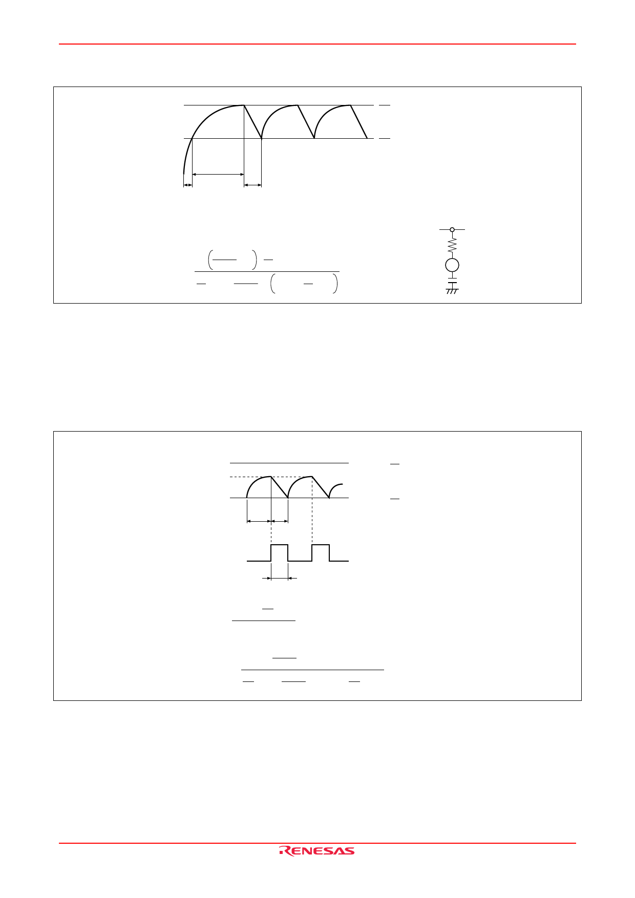
1. Pin(2) (TC pin) charge time and discharge time
When input to WD pin is abnormal, TC pin output waveform is as shown below:
TC
0V
tWD
tRST(1)
tRST(2)
4
5
⋅ VCC
2
5
⋅ VCC
∗ Please set it within the range
of 10kΩ ≤ R1 ≤ 30kΩ.
tRST(1) = 0.51 ⋅ C ⋅ R1
tWD = 1.1 ⋅ C ⋅ R1 (charge time)
tRST(2) = 1000 ⋅ C ⋅ ln
R1
1000
+1
⋅
4
5
⋅
VCC
–
VCC
2
5
VCC ⋅
R1
1000
–
VCC –
2
5
VCC
(discharge time)
Figure 3
Please set the time of tWD and tRST(2) within the following range.
110 µs ≤ tWD ≤ 1.1 s
8.3 µs ≤ tRST(2) ≤ 83 ms
VCC
R1
2
C
2. Pin (1) (WD pin) input frequency, input pulse width, charge time and discharge time
When input to WD pin is normal, TC pin output waveform is as shown below:
Pin (2) xV
t1 t2
(VCC = 3V)
2.4V
(= 4
5
⋅ VCC)
1.2V
(= 2
5
⋅ VCC)
Input
tWDIN
t1 = C ⋅ R1 ⋅ ln
VCC –
2
5
VCC
VCC – x
(charge time)
t2 = 1000 ⋅ C ⋅ ln
( R1
1000
+
1) ⋅ x
– VCC
2
5
VCC ⋅
R1
1000
– (VCC –
2
5
VCC)
(discharge time)
Figure 4
REJ03D0786-0200 Rev.2.00 Jun 15, 2007
Page 6 of 11
Share Link: 