MC10H181 查看數據表(PDF) - ON Semiconductor
零件编号
产品描述 (功能)
生产厂家
MC10H181 Datasheet PDF : 8 Pages
| |||
MC10H181
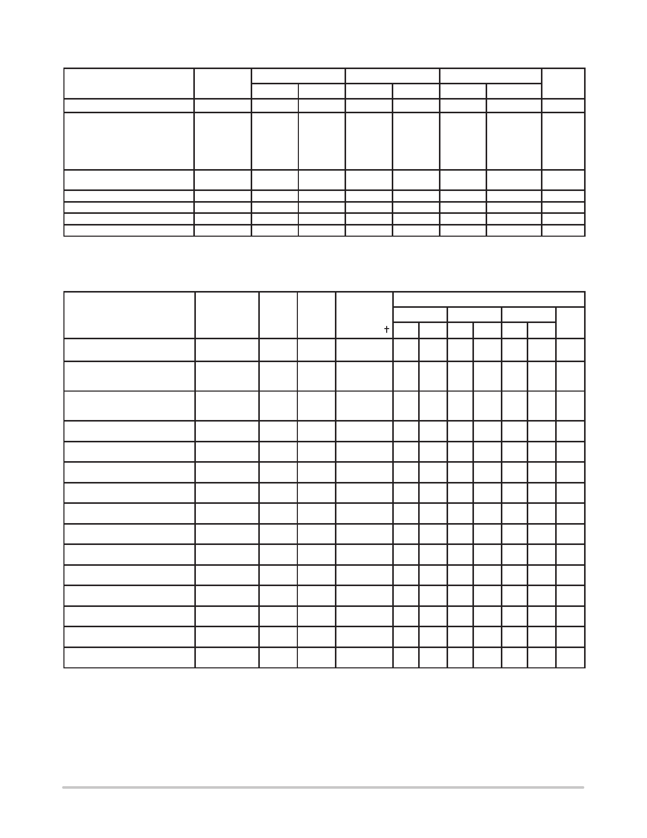
ELECTRICAL CHARACTERISTICS (VEE = –5.2 V ±5.0%) (See Note 1.)
0°
+25°
+75°
Characteristic
Symbol
Min
Max
Min
Max
Min
Max
Unit
Power Supply Current
Input Current High
Pin 22
Pins 14,23
Pins 13,15,17
Pins 10,16,18,21
Pins 9,11,19,20
IE
–
159
–
145
–
159
mA
IinH
µA
–
720
–
450
–
450
–
405
–
255
–
255
–
515
–
320
–
320
–
475
–
300
–
300
–
465
–
275
–
275
Input Current Low
Pins 9–11, 13–22
IinL
0.5
–
0.5
–
0.3
–
µA
High Output Voltage
Low Output Voltage
High Input Voltage
Low Input Voltage
VOH
VOL
VIH
VIL
–1.02
–0.84
–0.98
–0.81
–0.92
–0.735
Vdc
–1.95
–1.63
–1.95
–1.63
–1.95
–1.60
Vdc
–1.17
–0.84
–1.13
–0.81
–1.07
–0.735
Vdc
–1.95
–1.48
–1.95
–1.48
–1.95
–1.45
Vdc
1. Each MECL 10H series circuit has been designed to meet the dc specifications shown in the test table, after thermal equilibrium has been
established. The circuit is in a test socket or mounted on a printed circuit board and transverse air flow greater than 500 Ifpm is maintained.
Outputs are terminated through a 50–ohm resistor to –2.0 volts.
AC PARAMETERS
AC Switching Characteristics
0°C
+25°C
+75°C
Characteristic
Symbol
Input Output Conditions Min Max Min Max Min Max Unit
Propagation Delay
Rise Time, Fall Time
Propagation Delay
Rise Time, Fall Time
Propagation Delay
Rise Time, Fall Time
t+ +, t– –
t+, t–
t+ +, t+ –,
t– +, t– –
t+, t–
t+ +, t+ –,
t– +, t– –
t+, t–
Cn
Cn+4
A0,A1,A2,A3 0.7
2.0
0.7
2.0
0.7
2.2
ns
Cn
Cn+4
A0,A1,A2,A3 0.6
2.0
0.6
2.0
0.7
2.2
ns
Cn
F1
Cn
F1
Cn
F1
A0
ns
1.0 3.0 1.0 3.0 1.2 3.3
0.7 2.2 0.7 2.2 0.7 2.4
A1
F1
ns
A1
F1
1.5 3.7 1.5 3.7 1.6 4.0
A1
F1
0.7 2.0 0.7 2.0 0.7 2.2
Propagation Delay
Rise Time, Fall Time
Propagation Delay
Rise Time, Fall Time
Propagation Delay
Rise Time, Fall Time
Propagation Delay
Rise Time, Fall Time
Propagation Delay
Rise Time, Fall Time
Propagation Delay
Rise Time, Fall Time
Propagation Delay
Rise Time, Fall Time
Propagation Delay
Rise Time, Fall Time
t+ +, t– –
t+, t–
t+ +, t– –
t+, t–
t+ –, t– +
t+, t–
t+ +, t– +
t+, t–
t+ +, t– –
t+, t–
t+ +, t– –
t+, t–
t+ –, t– +
t+, t–
t+ +, t+ –
t+, t–
A1
PG
A1
PG
S0,S3
S0,S3
1.5 3.7 1.5 3.7 1.6 4.0
ns
0.9 2.4 0.9 2.4 0.9 2.6
ns
A1
GG
A0,A2,A3,Cn 1.5 3.7 1.5 3.7 1.6 3.9
ns
A1
GG
A0,A2,A3,Cn 0.7 2.2 0.7 2.2 0.7 2.4
ns
A1
Cn+4 A0,A2,A3,Cn 1.5 3.6 1.5 3.6 1.6 3.9
ns
A1
Cn+4 A0,A2,A3,Cn 0.5 2.0 0.5 2.0 0.5 2.2
ns
B1
F1
B1
F
S3,Cn
S3,Cn
2.0 4.5 2.0 4.5 2.1 4.8
ns
0.7 2.3 0.7 2.3 0.7 2.5
ns
B1
PG
B1
PG
S0,A1
S0,A1
1.5 3.8 1.5 3.8 1.6 4.0
ns
0.7 2.2 0.7 2.2 0.7 2.4
ns
B1
GG
B1
GG
S3,Cn
S3,Cn
1.5 3.7 1.5 3.7 1.6 4.0
ns
0.7 2.2 0.7 2.2 0.7 2.4
ns
B1
Cn+4
B1
Cn+4
S3,Cn
S3,Cn
2.0 4.0 2.0 4.0 2.1 4.3
ns
0.5 2.0 0.5 2.2 0.5 2.2
ns
M
F1
–
1.5 4.2 1.5 4.2 1.6 4.5
ns
M
F1
–
0.8 2.3 0.8 2.3 0.8 2.5
ns
Propagation Delay
Rise Time, Fall Time
t+ –, t– +
t+, t–
S1
F1
S1
F1
A1,B1
A1,B1
1.5 4.5 1.5 4.5 1.6 4.8
ns
0.7 2.0 0.7 2.0 0.7 2.2
ns
Propagation Delay
Rise Time, Fall Time
Propagation Delay
Rise Time, Fall Time
Propagation Delay
Rise Time, Fall Time
t– +, t+ –
t+, t–
t+ –, t– +
t+, t–
t+ –, t– +
t+, t–
S1
PG
S1
PG
S1
Cn+4
S1
Cn+4
S1
GG
S1
GG
A3,B3
A3,B3
A3,B3
A3,B3
A3,B3
A3,B3
1.5 4.0 1.5 4.0 1.6 4.3
ns
0.7 2.0 0.7 2.2 0.7 2.4
ns
1.5 4.1 1.5 4.1 1.6 4.4
ns
0.7 2.2 0.7 2.2 0.7 2.4
ns
1.3 4.5 1.3 4.5 1.4 4.8
ns
0.5 3.2 0.5 3.2 0.5 3.4
ns
† Logic high level (+1.11 Vdc) applied to pins listed. All other input pins are left floating or tied to +0.31 Vdc.
VCC1 = VCC2 = +2.0 Vdc, VEE = –3.2 Vdc
http://onsemi.com
4
Share Link: 