1SMCXXXAT3 查看數據表(PDF) - ON Semiconductor
零件编号
产品描述 (功能)
生产厂家
1SMCXXXAT3 Datasheet PDF : 8 Pages
| |||
1SMC5.0AT3 Series
MAXIMUM RATINGS
Rating
Symbol
Value
Peak Power Dissipation (Note 1.) @ TL = 25°C, Pulse Width = 1 ms
DC Power Dissipation @ TL = 75°C
Measured Zero Lead Length (Note 2.)
Derate Above 75°C
Thermal Resistance from Junction to Lead
DC Power Dissipation (Note 3.) @ TA = 25°C
Derate Above 25°C
Thermal Resistance from Junction to Ambient
PPK
PD
RqJL
PD
RqJA
1500
4.0
54.6
18.3
0.75
6.1
165
Forward Surge Current (Note 4.) @ TA = 25°C
IFSM
200
Operating and Storage Temperature Range
TJ, Tstg
–65 to +150
1. 10 X 1000 ms, non–repetitive
2. 1″ square copper pad, FR–4 board
3. FR–4 board, using ON Semiconductor minimum recommended footprint, as shown in 403 case outline dimensions spec.
4. 1/2 sine wave (or equivalent square wave), PW = 8.3 ms, duty cycle = 4 pulses per minute maximum.
Unit
W
W
mW/°C
°C/W
W
mW/°C
°C/W
A
°C
ELECTRICAL CHARACTERISTICS (TA = 25°C unless
otherwise noted, VF = 3.5 V Max @ IF = 100 A) (Note 5.)
Symbol
Parameter
IPP
Maximum Reverse Peak Pulse Current
VC
Clamping Voltage @ IPP
VRWM Working Peak Reverse Voltage
IR
Maximum Reverse Leakage Current @ VRWM
VBR
Breakdown Voltage @ IT
IT
Test Current
IF
Forward Current
VF
Forward Voltage @ IF
5. 1/2 sine wave or equivalent, PW = 8.3 ms
non–repetitive duty cycle
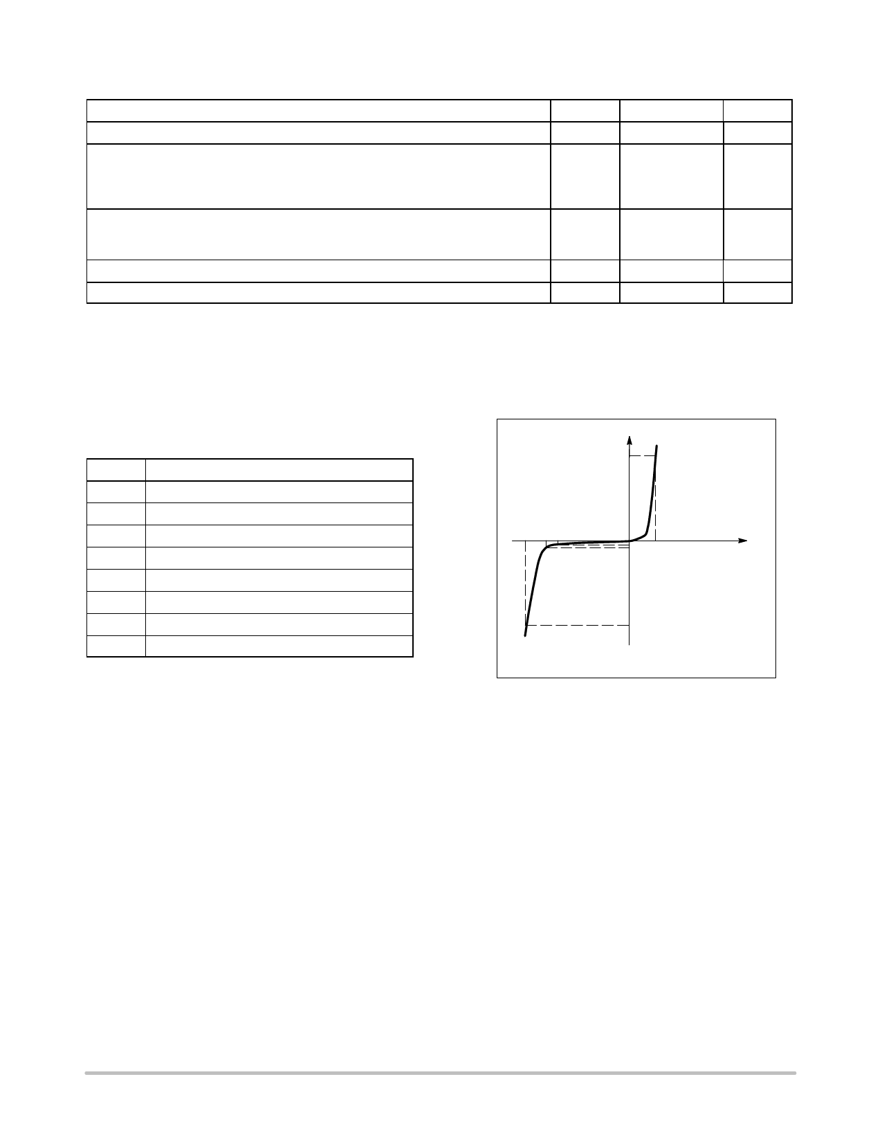
I
IF
VC VBR VRWM
IIRT VF
V
IPP
Uni–Directional TVS
http://onsemi.com
2
Share Link: 