MJ11033 查看數據表(PDF) - Motorola => Freescale
零件编号
产品描述 (功能)
生产厂家
MJ11033 Datasheet PDF : 4 Pages
| |||
ÎÎÎÎÎÎÎÎÎÎÎÎÎÎÎÎÎÎÎÎÎÎÎÎÎÎÎÎÎÎÎÎÎÎÎÎÎÎÎÎÎÎÎÎÎÎÎÎÎÎÎÎÎÎÎÎÎÎÎÎÎÎÎÎÎÎÎÎ MJ11028 MJ11030 MJ11032 MJ11029 MJ11031 MJ11033
ÎÎÎÎÎÎÎÎÎÎÎÎÎÎÎÎÎÎÎÎÎÎÎÎÎÎÎÎÎÎÎÎÎÎ ELECTRICAL CHARACTERISTICS (TC = 25_C unless otherwise noted)
ÎÎÎÎÎÎÎÎÎÎÎÎÎÎÎÎÎÎÎÎÎÎÎÎÎÎÎÎÎÎÎÎÎÎ Characteristic
Symbol
Min
ÎÎÎÎÎÎÎÎÎÎÎÎÎÎÎÎÎÎÎÎÎÎÎÎÎÎÎÎÎÎÎÎÎÎ OFF CHARACTERISTICS
ÎÎÎÎÎÎÎÎÎÎÎÎÎÎÎÎÎÎÎÎÎÎÎÎÎÎÎÎÎÎÎÎÎÎ Collector–Emitter Breakdown Voltage (1)
ÎÎÎÎÎÎÎÎÎÎÎÎÎÎÎÎÎÎÎÎÎÎÎÎÎÎÎÎÎÎÎÎÎÎ (IC = 1 00 mAdc, IB = 0)
MJ11028, MJ11029 V(BR)CEO
60
MJ11030, MJ11031
90
MJ11032, MJ11033
120
ÎÎÎÎÎÎÎÎÎÎÎÎÎÎÎÎÎÎÎÎÎÎÎÎÎÎÎÎÎÎÎÎÎÎ Collector–Emitter Leakage Current
ÎÎÎÎÎÎÎÎÎÎÎÎÎÎÎÎÎÎÎÎÎÎÎÎÎÎÎÎÎÎÎÎÎÎ (VCE = 60 Vdc, RBE = 1 k ohm)
(VCE = 90 Vdc, RBE = 1 k ohm)
ÎÎÎÎÎÎÎÎÎÎÎÎÎÎÎÎÎÎÎÎÎÎÎÎÎÎÎÎÎÎÎÎÎÎ (VCE = 120 Vdc, RBE = 1 k ohm)
ÎÎÎÎÎÎÎÎÎÎÎÎÎÎÎÎÎÎÎÎÎÎÎÎÎÎÎÎÎÎÎÎÎÎ (VCE = 60 Vdc, RBE = 1 k ohm, TC = 150_C)
(VCE = 90 Vdc, RBE = 1 k ohm, TC = 150_C)
ÎÎÎÎÎÎÎÎÎÎÎÎÎÎÎÎÎÎÎÎÎÎÎÎÎÎÎÎÎÎÎÎÎÎ (VCE = 120 Vdc, RBE = 1 k ohm, TC = 150_C)
ÎÎÎÎÎÎÎÎÎÎÎÎÎÎÎÎÎÎÎÎÎÎÎÎÎÎÎÎÎÎÎÎÎÎ Emitter Cutoff Current (VBE = 5 Vdc, IC = 0)
ÎÎÎÎÎÎÎÎÎÎÎÎÎÎÎÎÎÎÎÎÎÎÎÎÎÎÎÎÎÎÎÎÎÎ Collector–Emitter Leakage Current (VCE = 50 Vdc, IB = 0)
ON CHARACTERISTICS (1)
ICER
MJ11028, MJ11029
—
MJ11030, MJ11031
—
MJ11032, MJ11033
—
MJ11028, MJ11029
—
MJ11030, MJ11031
—
MJ11032, MJ11033
—
IEBO
—
ICEO
—
ÎÎÎÎÎÎÎÎÎÎÎÎÎÎÎÎÎÎÎÎÎÎÎÎÎÎÎÎÎÎÎÎÎÎ DC Current Gain
ÎÎÎÎÎÎÎÎÎÎÎÎÎÎÎÎÎÎÎÎÎÎÎÎÎÎÎÎÎÎÎÎÎÎ (IC = 25 Adc, VCE = 5 Vdc)
ÎÎÎÎÎÎÎÎÎÎÎÎÎÎÎÎÎÎÎÎÎÎÎÎÎÎÎÎÎÎÎÎÎÎ (IC = 50 Adc, VCE = 5 Vdc)
Collector–Emitter Saturation Voltage
ÎÎÎÎÎÎÎÎÎÎÎÎÎÎÎÎÎÎÎÎÎÎÎÎÎÎÎÎÎÎÎÎÎÎ (IC = 25 Adc, IB = 250 mAdc)
ÎÎÎÎÎÎÎÎÎÎÎÎÎÎÎÎÎÎÎÎÎÎÎÎÎÎÎÎÎÎÎÎÎÎ (IC = 50 Adc, IB = 500 mAdc)
ÎÎÎÎÎÎÎÎÎÎÎÎÎÎÎÎÎÎÎÎÎÎÎÎÎÎÎÎÎÎÎÎÎÎ Base–Emitter Saturation Voltage
(IC = 25 Adc, IB = 200 mAdc)
ÎÎÎÎÎÎÎÎÎÎÎÎÎÎÎÎÎÎÎÎÎÎÎÎÎÎÎÎÎÎÎÎÎÎÎÎÎÎÎÎÎÎÎÎÎÎÎÎÎÎÎÎÎÎÎÎÎÎÎÎÎÎÎÎÎÎÎÎ v v (IC=50Adc,IB=300mAdc)
(1) Pulse Test: Pulse Width 300 µs, Duty Cycle 2.0%.
hFE
1k
400
VCE(sat)
—
—
VBE(sat)
—
—
Max
Unit
—
Vdc
—
—
mAdc
2
2
2
10
10
10
5
mAdc
2
mAdc
—
18 k
—
Vdc
2.5
3.5
Vdc
3.0
4.5
100
50
20
10
5
2
1
0.5
0.2
0.1
0.2
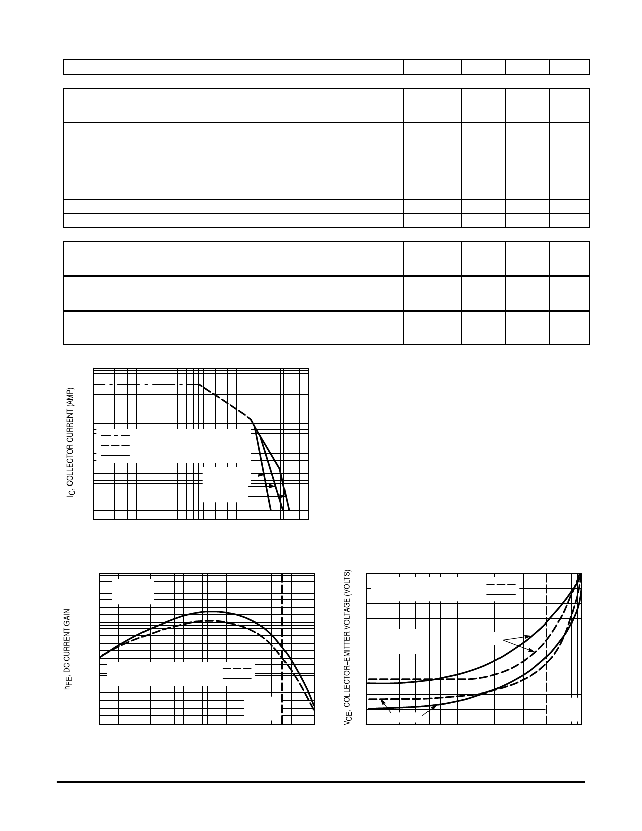
BONDING WIRE LIMITED
THERMALLY LIMITED @ TC = 25°C
SECOND BREAKDOWN LIMITED
MJ11028, 29
MJ11030, 31
MJ11032, 33
0.5 1 2
5 10 20
50 100 200
VCE, COLLECTOR–EMITTER VOLTAGE (VOLTS)
There are two limitations on the power–handling ability of a
transistor: average junction temperature and second break-
down. Safe operating area curves indicate IC – VCE limits of
the transistor that must be observed for reliable operation,
i.e., the transistor must not be subjected to greater dissipa-
tion than the curves indicate.
The data of Figure 2 is based on TJ(pk) = 200_C; TC is
variable depending on conditions. At high case tempera-
tures, thermal limitations will reduce the power that can be
handled to values less than the limitations imposed by se-
cond breakdown.
Figure 2. DC Safe Operating Area
100 k
50 k
20 k
VCE = 5 V
TJ = 25°C
5
MJ11029, MJ11031, MJ11033 PNP
MJ11028, MJ11030, MJ11032 NPN
4
10 k
5k
2k
1k
MJ11029, MJ11031, MJ11033 PNP
MJ11028, MJ11030, MJ11032 NPN
500
200
100
1
2
80 µs
(PULSED)
5
10
20
50
100
3
TJ = 25°C
IC/IB = 100
2
1
0
VCE(sat)
1
23
5
VBE(sat)
10
20
80 µs
(PULSED)
50
100
IC, COLLECTOR CURRENT (AMP)
IC, COLLECTOR CURRENT (AMP)
Figure 3. DC Current Gain
Figure 4. “On” Voltage
2
Motorola Bipolar Power Transistor Device Data
Share Link: 